
Intel Core 2 Extreme QX9650
Manufacturer: IntelUK Price (as reviewed): around £650 (inc. VAT)
US Price (as reviewed): around $999 (ex. Tax)
Back at IDF in September, Intel CEO Paul Otellini announced that the chip giant’s first 45nm processor would be launched on the 12th November. That day is less than two weeks away now but today we can finally unveil some independent performance numbers on Intel’s new flagship processor, the Core 2 Extreme QX9650.
As an Extreme Edition processor, it not surprisingly carries the same $999 USD per chip in 1,000 unit quantities price tag as its predecessor, the Core 2 Extreme QX6850, meaning that it’ll probably set you back somewhere between £650 and £700 (inc. VAT) at your favourite e-tailer. If that’s well out of your price range, fear not because Intel will be launching some lower-priced alternatives at the start of next year.
For now though, we’ve got the QX9650 in-hand, which comes clocked at the same 3GHz clock speed as the QX6850 it’s replacing. It also uses the same 1,333MHz front side bus too, but there’s more to CPU performance than just raw clock speed – we’ve known that since long before the days of Pentium 4. The Penryn family is no exception to this rule and there are changes – some quite significant – in, well... most things. Let’s have a look at what’s changed before we get onto how the QX9650 performs.
Error 404: atomic layers not found
For some time, many have worried that we’d eventually reach the point when Moore’s Law will no longer be applicable because the laws of physics gets in the way. One point where some believed the law, which has been heavily modified since its inception, would come unstuck was with the move to a 45-nanometre manufacturing process.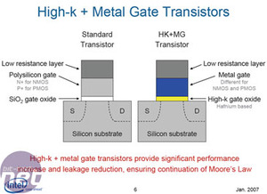
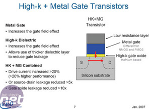
The reason for this is that Intel has used a silicon dioxide insulator inside its transistors for around 15 years now, but with the vast improvements in manufacturing technology since then, the chip manufacturer hit a wall when it got to 65 nanometres. The silicon dioxide gate dielectric was just five atomic layers thick and as the wall gets thinner, the amount of current leakage increases. If Intel had moved to a 45nm process using silicon dioxide gate dielectric walls, there could have been a situation where the transistors would never be fully switched off, making for a very power inefficient microprocessor.
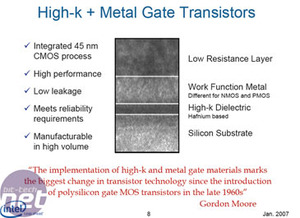
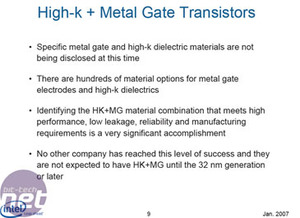
To combat this problem, Intel’s advanced research and development team set out to redesign the transistor because at some point the chip manufacturer would simply run out of atoms. The result of this research was the hafnium-based high-k metal gate transistor, something that most regular bit-tech readers will be familiar with after we covered the technology in some depth back in January.
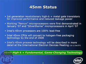
The main benefits of this technology are a 20 percent faster switching speed in the same power envelope and a 30 percent power reduction at the transistor level. While the research started at the University of Tokyo, with the invention of the hafnium based high-k dielectric, Intel has remained very tight lipped as to what the new PMOS and NMOS transistors are made of.
But what does "high-k" actually mean?
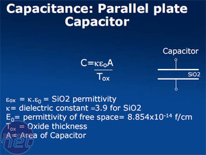
I know, it's early in the morning for us Brits, but it's time for some mathematics, I'm afraid. Take a look at the equation below - the overall capacitance of the transistor is equal to the dielectric constant, which is 3.9 for normal traditional Silicon Dioxide, multiplied by the permittivity of free space (also a constant) and the area of the capacitor; this is all divided by the Silicon Oxide's thickness.Basically, by keeping the capacitor value the same, you can increase the dielectric constant by using the Hafnium Oxide based material instead of Silicon Dioxide, which also means you can increase the Oxide thickness (Tox) too. This increase in dielectric constant means you've now got a "high-k" material.
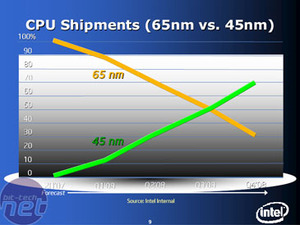
Intel has ramped up its 45-nanometre production in two factories – D1D in Oregon and Fab 32 in Arizona. A third, Fab 28 in Israel, will come online in the first half of 2008 and a fourth, Fab 11X in Mexico, is expected to come online sometime in the second half of 2008.
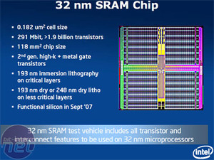
Intel's research on its 32nm process is also well under way, as Paul Otellini showed off a wafer of 219 Mbit SRAM cells featuring 1.9 billion transistors and a 1.9x density increase over 45nm at IDF last month. For what it's worth, 32nm processors aren't due until the end of 2009 with the Nehalem refresh, Westmere, so there's quite a way to go yet.

MSI MPG Velox 100R Chassis Review
October 14 2021 | 15:04



Want to comment? Please log in.