Nvidia GeForce GTX 580 Review
Manufacturer NvidiaUK price (as reviewed) Around £399 (inc VAT)
US price (as reviewed) Unknown
GeForce GTX 580 1.5GB specifications
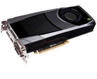
Nvdia had significant trouble releasing the first GF100 Fermi-based GPU back in March, with launch delays letting ATI rule the DX11 battleground for roughly six months. It didn’t help that when the GeForce GTX 480 1.5GB did find its way to our test rigs, it wasn’t fast enough for the price, and also ran hot, loud and consumed too much power. What a difference a few months make, as the new GeForce GTX 580 1.5GB solves all of these issues.
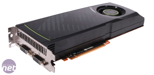
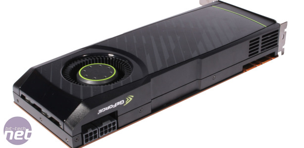
We’ve leave the GeForce GTX 580 1.5GB performance analysis till after the benchmarks, and instead talk about the upgrades that the GPU and the reference card have received on this and the next page.
GPU Upgrades
While Nvidia has made the obvious move of unlocking the 16th and final SM (Streaming Multiprocessor, or ‘stream processor cluster’ in neutral terminology) of the GF100 architecture for the GeForce GTX 580 1.5GB, the new GF110 codename reveals that this isn’t the full extent of the changes. The most significant difference between GF110 and GF100 is the use of different grades of transistor.Typically a GPU will use the fastest switching transistors to attain the highest possible frequencies, but these transistors are also the most leaky, resulting in higher power consumption and more waste heat. With the GF110 design, Nvidia has used less leaky transistors for non-performance-critical areas of the GPU, thus lowering the overall power draw of the chip.
However, the power-saving transistors – despite their slower switching tendencies – haven’t lead to a lower GPU frequency for the GeForce GTX 580 1.5GB. The GTX 580 1.5GB’s GPU core operates at 772MHz rather than the 700MHz of the GeForce GTX 480 1.5GB, with the 512 stream processors ripping along at 1,544MHz rather than 1,400MHz.
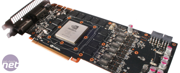
Nvidia has also added temperature and power draw monitoring to the GeForce GTX 580 1.5GB via two additional chips on the card. This means that if the GPU or the card’s VRMs get too hot or try to draw more power than is safe, the GPU will clock down to avoid damage to the hardware.
There are three things to note about this power management technology, the first being that as it’s enabled by two separate chips on the card - board partners can choose to leave them off to lower the cost of their card. Secondly, the GPU won’t increase in frequency if the power draw or temperature are lower than the maximums – the technology is more akin to Intel’s SpeedStep than Turbo Boost. Finally, the monitoring is software-based and at the moment only detects OCCT and the latest version of FurMark. This means that any thermal or power draw test using these applications are inaccurate, but as we use 3DMark06 to stress the GPUs, our numbers are perfect.
While a hardware-only implementation of power monitoring might be preferable – it would be automatic, based on the actual power draw or temperature of the components, and not be dependent on driver interaction – Nvdia said that actually a software-based implementation had more advantages. It allows Nvidia to be more flexible, letting Nvidia add extra applications that it finds to be particularly power hungry. However, the option to disable power monitoring isn't exposed in the driver, so extreme overclockers and anyone wanting to verify that their card is working properly and not overheating will have to be careful.
Apart from the unlocked SM, the GPU has seen its high-precision fp16 capabilities increased, which Nvidia claims improves performance by 4-12 per cent alone. We look at the revamped, full-fat Fermi architecture on the next page.

MSI MPG Velox 100R Chassis Review
October 14 2021 | 15:04




Want to comment? Please log in.