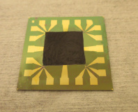
I don't know what it is about the run up to Christmas this year, but it seems like every researcher in the world has a new scheme for ultra-fast processors that they're just itching to tell us. The latest plan comes courtesy of Princeton University boffins who have developed a system of putting transistors on a 'graphene' substrate – carbon formed into a honeycomb lattice.
Graphene-based processors promise – you guessed it – massive advantages in performance and power usage over traditional silicon-based chips. The reason we haven't been using it in the past is due to the difficulties in arranging graphene into a layer which is the right size to make chips out of. A standard silicon wafer used in the production of processors is between eight and twelve inches in diameter, and currently they can't get a slab of graphene anywhere near that.
Stephen Chou, professor of electrical engineering, reckons his team has the solution to the problem: put the graphene “only in the active areas of the chip”, which neatly side-steps the whole too-small problem.
The actual process used is described by Chou as being “like printing”, where a special stamp is pressed against a graphite block and then used to transfer layers just a few atoms thick to the wafer on which the transistors will be built. Like potato-printing, but on a teeny-tiny scale and with extremely expensive potatoes.
The researchers think the new technology could rapidly find its way into devices which “require high-power output” such as mobile 'phones. As usual, the sticking point is in scaling the technology to a level at which commercialisation becomes possible.
Do you think the technology holds promise, or will you believe it when you see it? Let us know via the forums.

MSI MPG Velox 100R Chassis Review
October 14 2021 | 15:04


Want to comment? Please log in.