
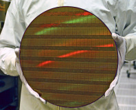
Intel, Samsung Electronics and TSMC have reached an agreement to push forwards with plans to move semiconductor manufacturing to 450mm wafers starting in 2012.
The trio say that they’ll cooperate with the rest of the semiconductor industry to ensure that all of the required components, infrastructure and capability are developed in readiness for a 450mm pilot line in 2012.
The first 300mm wafer production began in 2001, ten years after the first 200mm wafers started to come off the production line. The transition to 450mm wafers will take a little longer than past-history dictates, but the trio say that because of the complexity involved in such a move, the target date will be constantly evaluated, as it will be “critical to ensure industry-wide readiness.”
"Increasing cost due to the complexity of advanced technology is a concern for the future," said Mark Liu, TSMC's senior vice president of Advanced Technology Business. "Intel, Samsung, and TSMC believe the transition to 450mm wafers is a potential solution to maintain a reasonable cost structure for the industry."
A 450mm wafer has over twice the surface area of a 300mm wafer and Intel says that the increased efficiency associated with a move to a larger wafer size will also help to reduce the overall resource usage (energy, water, etc) in every chip. Moving to larger wafers will no doubt to lower the cost of production per chip, and this should help to keep costs reasonable and also potentially open the market to a broader audience.
It’s quite possible that we won’t see products manufactured on 450mm wafers for a few years after the transition starts, but we’re excited to see how what doors this move opens for the semiconductor industry. Discuss in the forums.
RELATED ARTICLES


MSI MPG Velox 100R Chassis Review
October 14 2021 | 15:04

Want to comment? Please log in.