
French tech site Hardware.fr seems to have taken the only photo of Intel Senior VP, Pat Gelsinger, at IDF in Beijing, showing off Larabee.
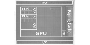
PC Perspective claims to count 64 dies in the picture, which means even at full yield (it never happens) that would be a very costly part. This is on the assumption that Intel's Gelsinger is holding up a recent die made on 45nm, and not an older one made on 65nm, as there were some claims last year of early samples being used internally on the older process.
Attempting to calculate the die size (on the heavy assumption that it's square) we think Larrabee is a massive 700mm die. To work this out, we first jimmied the levels of the image in Adobe Photoshop, and could just about make out there are eight cores almost exactly in a diagonal. Assuming Gelsinger is holding a 300mm wafer, that equates to 37.5mm per diagonal, or 26.5mm a side. 26.5 squared therefore makes 702.25 mm² total area.
In his article on the French site, writer Damien Triolet claims a die size of "approximately 600mm²" however. Either way, 600-700mm² has people claiming somewhere in the region of 1.6-1.7Bn transistors.
In comparison, Nvidia's GT200 was 576mm at 1.4Bn squared making Larrabee in the region of 4-22 percent larger on that wafer.
Another comparative - Intel Tukwila - is a 2 billion transistor Itanium chip at 712mm squared, however while Tukwila is mostly L3 cache, whereas Larrabee is small IA cores. It also depends on the core frequencies too, and whether it's electrical paths buffed out for extra frequency like the ATI Radeon HD 4890 versus 4870 for example?
The general consensus claims Intel will launch its super sized part on 45nm - the largest to date on High-K Metal Gate, however since the process is mature this will give more security for a larger die. The 45nm High-K MG will lower power and leakage quite considerably, but it depends on the actual transistor and "core" count, as well as power/clock gating, versus aforementioned frequency fattening and IO routing: basically there are too many factors still outstanding for firm conclusions.
What do you think? Big and hot or the next super seller? What do you make the die-size to be? Let us know your thoughts and calculations in the forums!


MSI MPG Velox 100R Chassis Review
October 14 2021 | 15:04

Want to comment? Please log in.