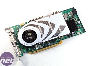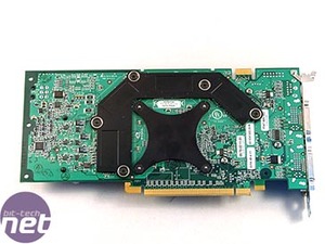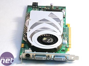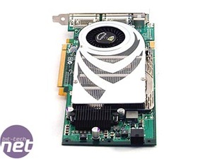

GeForce 7800 GTX is the first video card in the GeForce 7 series, and it is based on a 0.11-micron TSMC manufacturing process. This is the same process that was used for GeForce 6600 series, and GeForce 6200 series initially. It was then followed by NV41, which is the chip behind GeForce 6800 Std and GeForce 6800 LE. Finally, NV42, the chip behind GeForce Go 6800 Ultra, was released towards the back end of last year. Note that the chips are getting more and more complex as time goes by on this process – it allows NVIDIA to get the process right before creating their next-generation high end part on that manufacturing process.
It has 24 internal pixel pipelines, 8 vertex shaders and a 256-bit memory interface. In much the same way as the GeForce 6600 series, the pixel output engines (ROPs) are completely orthogonal, and despite there being 24 pixel pipelines, there are only 16 pixel output engines. We feel that this is a smart move by NVIDIA, and it allows the 16 ROPs in G70 to have a higher efficiency than those in NV40 and NV45.


The GPU is a native PCI-Express graphics processor, and thus has support for SLI – the heatsink at the end of the card is cooling the voltage regulators, and not a HSI bridge chip. SLI support is improving over time, and this driver release sees the addition of another twenty profiles that are predefined by the driver. You can, of course, add your own SLI profiles in order to make games work that don't have an optimised SLI profile created for them just yet.


MSI MPG Velox 100R Chassis Review
October 14 2021 | 15:04


Want to comment? Please log in.