
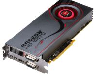
ATI Radeon HD 5850 Power Circuit
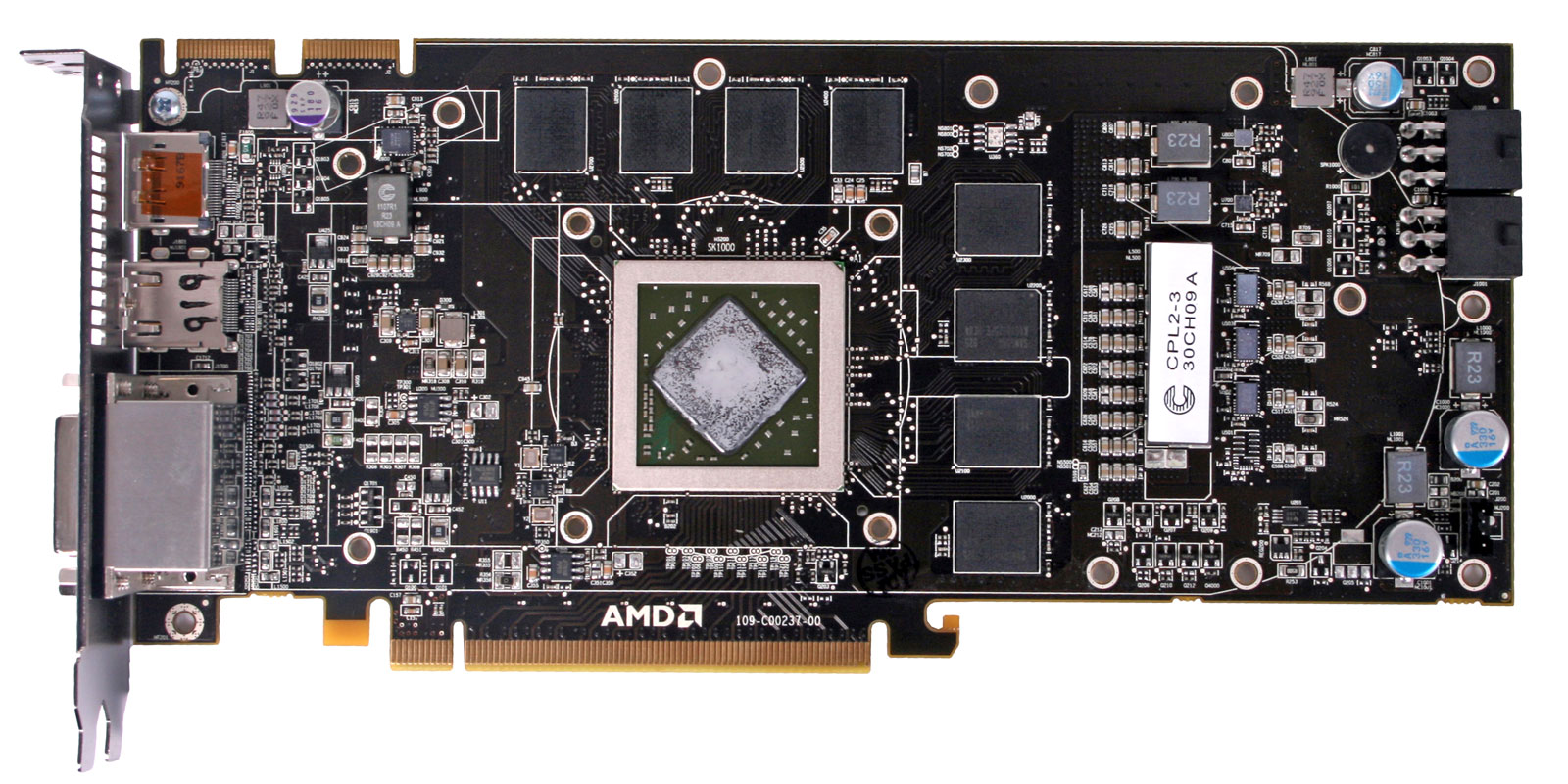
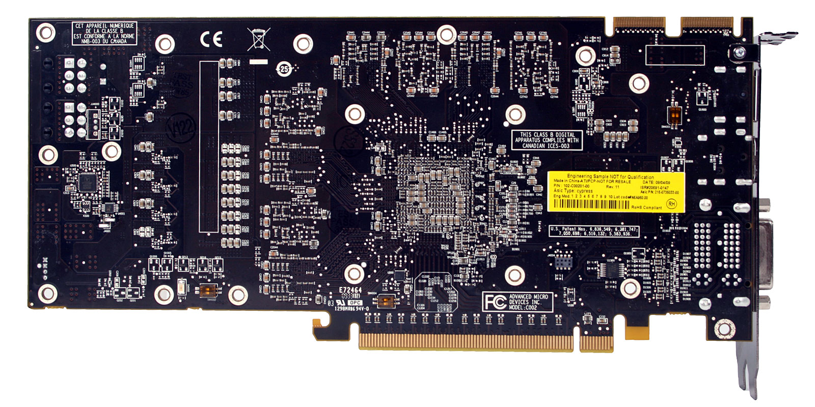
As with all the other boards in AMD's new Radeon HD 5000 series, we've taken a look at how power is being delivered to the various parts of the card. We were particularly impressed by how robust the Radeon HD 5870's power circuit was, but that came at the expense of an over-sized PCB that won't easily fit into every chassis out there.Things are different with the Radeon HD 5850 however, as its 9in PCB is much more manageable for the masses. It is worth noting that the two PCI-E power connectors' positioning does mean that while the board is only 9 inches, you're going to have to factor in the room required for the power cables - we reckon you'll need to allow for at least an inch at the end of the card.
Given that the board still uses two 6-pin PCI-Express power connectors, there's an additional 150W of power available (both are required for the board to function) on top of the 75W through the PCI Express interconnect. Taking this into account, AMD says that the board consumes a maximum of 170W, which is a long way below the 225W maximum deliverable board power. While we're on the topic of power consumption, AMD says that the 5850's idle power is exactly the same as the 5870's, meaning the two disabled SIMD cores don't have any impact on power gating.
Click to enlarge
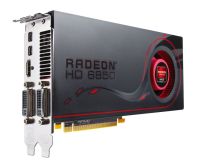
Under the heatsink, there are eight Samsung KG10325FE-HC04 GDDR5 memory chips - the same DRAMs that are on the Radeon HD 5870. They're rated to an impressive 1,250MHz (5,000MHz effective), so there should be some decent headroom available for overclocking providing AMD hasn't artificially hampered the 5850's memory (the power circuitry is all intact).
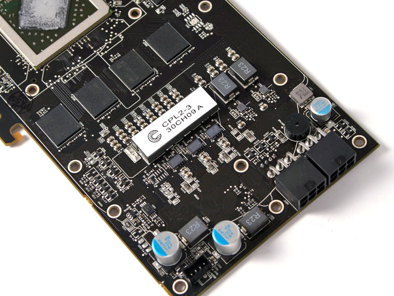
To continue the trend of costing down the Radeon HD 5850, the GPU's power is now delivered by three phases instead of the four included on the Radeon HD 5870's PCB, although AMD or its partners could release a derivative with four phases as there are solder points available for that fourth phase. We shouldn't forget that AMD could also beef up the Radeon HD 5870 GPU's power delivery too, as there is room to expand to a fifth phase for the GPU on its PCB.
Click to enlarge
The phases use the same Volterra VT1157SF PWMs, which are all controlled by the familiar Volterra VT1165MF voltage regulator - this is now relocated on the rear of the PCB in order to save some space. Additionally there are two Volterra VT242WF PWMs supplying power to the memory - another familiar sight carried over from the 5870.

Click to enlarge
Continuing our tour around the board, there's a lone phase (with no optional expansion for partners) which is presumably for the memory controller on the Cypress GPU. It uses a single VT237WF PWM, on which we've been able to find very little in the way of useful information. It appears to be both controlling and regulating voltage passing through the memory controller circuit though, as there isn't an easily identifiable VRM.
Let's get on and see how the card performs...


MSI MPG Velox 100R Chassis Review
October 14 2021 | 15:04

Want to comment? Please log in.