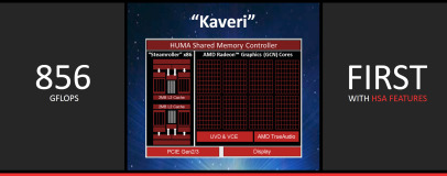
AMD has just kicked off its annual developer conference, APU13, and to get the ball rolling it has revealed a host of details about its upcoming APU, codenamed Kaveri, with the new chip set to arrive on 14 January 2014.
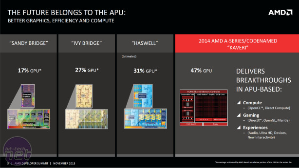
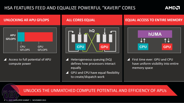
Kaveri will be the company's first chip to completely unify both CPU and GPU together on one chip, an approach AMD is calling Heterogeneous System Architecture (HSA).
The key to HSA is that both the CPU and GPU, for the first time, share the same memory space and have equal flexibility to create and dispatch workloads. This is in contrast to previous APUs that have required workloads that need GPU processing to be copied back and forth to the GPU memory space.
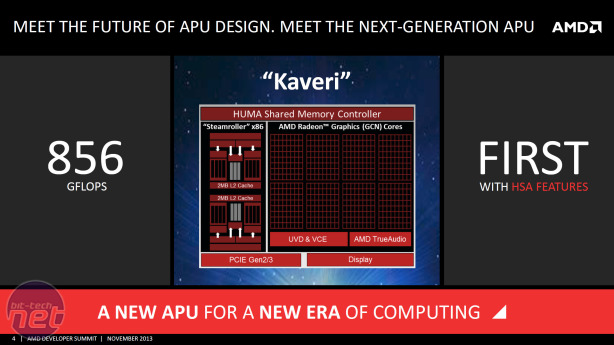
Also revealed are details of what the highest-spec chip will be. Kaveri will have up to 4 CPU cores (2 modules) that will be based on the company's existing CPU architecture, Steamroller. It will also feature a GPU composed of 8 GCN 1.1 Compute Units (CUs), making for a Stream Processor (SP) count of 512, or the equivalent of a Radeon HD 7750 desktop card.
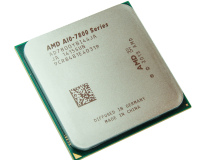
AMD claims these numbers equate to a floating point processing figure of 856GFLOPS, which Anandtech has worked out via PCWorld will mean it is called the A10-7850K, clocked at 3.7GHz and with a GPU speed of 720MHz.
Also confirmed are that AMD's proprietary GCN API, Mantle, will be supported by Kaveri and that its new TrueAudio technology will also be incorporated into the chip.
The January 14 launch will, in contrast to previous APU launches, be for desktop FM2+ chips first with mobile parts to follow soon after. The launch will be the week after the CES trade show, where AMD is expected to provide further details about the new chips, including pricing and specific SKUs.

MSI MPG Velox 100R Chassis Review
October 14 2021 | 15:04




Want to comment? Please log in.