Semiconductor foundry giant Samsung has announced that it is forging ahead with a 7nm low-power extreme ultraviolet (EUV) lithographic process it claims offers the choice between a 10 percent performance uplift or 35 percent power consumption drop compared to its 10nm FinFET process.
One of the many techniques employed to continue the struggling march of Moore's Law - the observation by Intel co-founder Gordon Moore that the number of transistors on a leading-edge chip tends to double every 18 months, requiring the size of said transistors to shrink lest we're left with processors the size of football fields - EUV lithography replaces the standard lightsource of photolithographic scanning with one operating at the extreme end of the ultraviolet spectrum. The result: a photolithographic scanner capable of laying down significantly finer patterns than traditional lasers, assisting with the shrink to a lower process node.
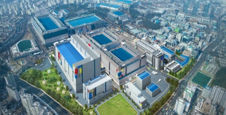
While Samsung first introduced its 7nm Low Power Plus (LPP) EUV lithographic process last May as part of a roadmap that included 8nm, 7nm, 6nm, 5nm, and 4nm nodes, the parts have not yet rolled off the production line. Following the promise of late-2018 production at the company's existing facilities in September last year, a ground-breaking ceremony held this week and hosted by Kinam Kim, president and chief executive of Samsung's Device Solutions arm, offered a deadline for completion of the company's first dedicated 7nm LPP fab: The facility will be finished by the second half of 2019, and production ramp-up will begin in 2020 - a target which will see Samsung investing $6 billion by the time the EUV line begins production at scale.
While the Hwaseong fab won't be churning out chips for another couple of years, it already has a customer: Samsung has confirmed that Qualcomm's future Snapdragon 5G mobile chipsets will be built on the 7nm LPP EUV process. Samsung credits the win to three key features of the 7nm LPP process over its current 10nm FinFET alternative: a simplified photolithographic process which improves yields, a 40 percent increase in area efficiency, and a choice of taking a 10 percent performance gain or a 35 percent reduction in power draw for any given design.
'We are pleased to continue to expand our foundry relationship with Qualcomm Technologies in 5G technologies using our EUV process technology,' claims Charlie Bae, Samsung's head of foundry sales and marketing. 'This collaboration is an important milestone for our foundry business as it signifies confidence in Samsung’s leading process technology.'


MSI MPG Velox 100R Chassis Review
October 14 2021 | 15:04

Want to comment? Please log in.