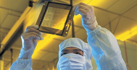
Taiwan Semiconductor (TSMC) has announced volume production on its new N7+ 7nm process node - the semiconductor industry's first commercially-available extreme ultraviolet (EUV) lithographic process, it claims.
The decades-long march of Moore's Law, long since upgraded from a simple observation by Intel co-founder Gordon Moore that the number of transistors on a leading-edge part trends towards a doubling every 18 months to a slavishly-followed design rule, has left the semiconductor industry reaching for ever-more esoteric manufacturing methods to keep feature sizes shrinking and transistor counts rising. The latest to be reaching volume production is extreme ultraviolet lithography (EUV), which uses light wavelengths around the 13.5nm mark at high energy levels to transfer considerably finer patterns than allowable with standard photolithography - and, as an added bonus, in a single mask.
EUV isn't a new technology - Intel invested in it back in 2012, while Samsung broke ground on a dedicated EUV fab in February 2018 and launched its first 7nm EUV process node in October the same year. Both Samsung and Taiwan Semiconductor, meanwhile, have boasted of EUV-powered process nodes of 5nm and 6nm respectively - but, thus far, neither have reached volume production status.
This week, TSMC announced it had begun volume shipping on what it claims is 'the industry's first commercially-available EUV lithography technology: N7+. An EUV variant of its existing N7 7nm process node, N7+ began production earlier this year with considerable success: TSMC claims it has matched the yield - the percentage of parts which are built to-spec to the parts which have faults - of the N7 part already, despite the non-EUV variant having been in volume production for over a year.
The N7+ process node offers advantages over its predecessor, TSMC claims: Density is increased 15 to 20 percent, and power consumption is lowered. The company is also using the same technology for N6, its promised 6nm EUV process node, which it claims will enter risk production in the first quarter of 2020 and volume production by the end of that year while boosting density a further 18 percent.
'With AI and 5G unlocking so many new ways for ICs to improve our lives, our customers are full of innovative leading-edge design ideas, and they are relying on TSMC's technology and manufacturing to make them real,' crows Dr. Kevin Zhang, TSMC vice president of business development. 'Our success in EUV is another great example of how TSMC not only makes those leading-edge designs possible, but also delivers in high volume with our manufacturing excellence.'
TSMC is currently the focus of a patent infringement suit filed by rival GlobalFoundries, to which it has responded with a countersuit alleging infringement of its own patents.


MSI MPG Velox 100R Chassis Review
October 14 2021 | 15:04

Want to comment? Please log in.