
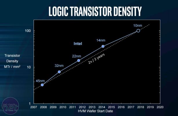
Moore’s law is one of the mainstays of the CPU world and has generally held true over the last 40 years when Intel co-founder Gordon Moore, forecast a doubling every two years of the number of components or transistors on an integrated circuit. Prior to this, progress was even faster, while moving to the present day paints perhaps a slightly more complicated picture; manufacturing processes are getting so tiny that progress comes at a higher cost.
It’s fair to say that many are of the opinion that Moore’s law is no longer in effect, or that Intel will fail to meet its requirements in the next generation or two of its CPUs – the company obviously deals with plenty of areas outside the desktop CPU market, but it’s that which we’re focussing on here. Whether this is due to the lack of competition in the desktop CPU marketspace over the last decade, or just people’s perception picturing a somewhat familiar and maybe monotonous launch cycles of Intel CPUs, it’s difficult to tell, but the company held a Technology and Manufacturing day in San Francisco to address the issue and bit-tech went along. It believes Moore’s law isn’t just alive and well, but that the company has actually been exceeding it.
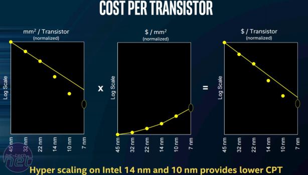
The last few years have seen new materials and new technologies such as tri-gate transistors help Intel to continue to push down the manufacturing process, which this year is likely to see the first 10nm parts. However, it’s thanks to hyper scaling that Intel has been able not just to get to the 10nm goal, but also to make it financially viable in terms of transistor cost.
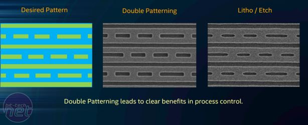
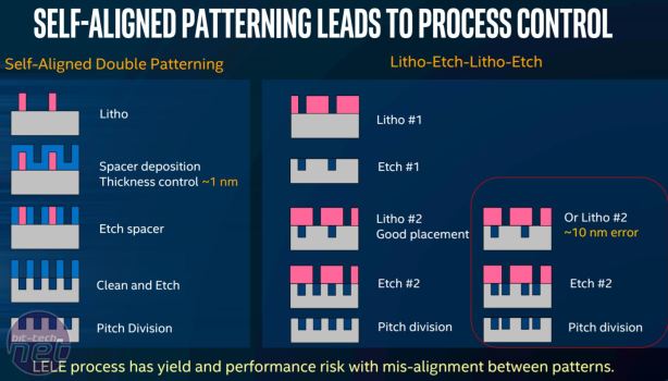
Hyper scaling – Intel’s term for a collection of new technologies that have made the move to 10nm possible, relies on enhanced patterning techniques and precision down to the 1nm scale for extremely precise control of the lithography. Intel has moved on from the traditional litho-etch-litho-etch process of creating transistors on the nanometre scale to a Self-Aligned Double Patterning technique for 14nm and more recently a Quad Patterning technique for 10nm – essentially multi-pass patterning schemes.
The transistor fin pitch has been aggressively scaled to allow over 10m transistors per square millimetre for the first time – fins are now 25 percent taller and more closely spaced compared to 14nm. Multiple pass patterning schemes are more expensive, yet Intel has actually reduced the cost per transistor thanks to a reduction in errors due to the more precise lithography leading to increased yields.
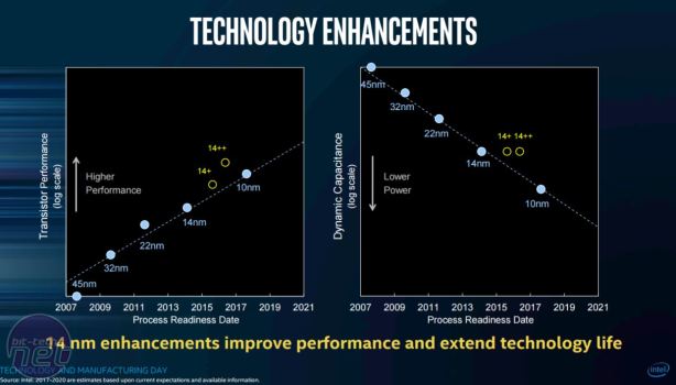
Intel’s new three-phase launch cycle, which moves away from the traditional tick-tock cycle of a move to a smaller manufacturing process (tick) to a new architecture (tock) also plays a key role in Moore’s law. It also may have resulted in many assuming that the cycle would mean Moore’s law would be impossible to adhere to. The additional costs of Hyper Scaling mean that it’s sensible for Intel to continue to improve a manufacturing node – there are other reasons too outside of CPU manufacturing, but refining the process has seen an increase of transistor performance as we moved from the first 14nm Intel desktop CPU (Broadwell), to the architectural redesign - Skylake and finally to Kaby Lake (14nm+).
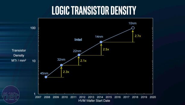
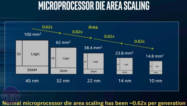
Hyper scaling is key here as it actually means that while the launch cycle is different to the tick/tock style we’re used to, with a longer time between moves from one node to another, the transistor density is actually increasing in bigger steps over the same amount of time. There may be three years between process node changes now, with a new CPU range each year, but with 14nm and later this year with 10nm in some areas, Intel is actually ahead of the Moore’s law prediction due to a more significant bump in transistor density.
Specifically with 10nm, Intel has introduced other new features, although it couldn’t go into too much detail. Contact over active gate allows a 10 percent reduction in the space required, while single dummy gate apparently allows 20 percent more area scaling. Combined they allow for a 2.7x increase in transistor density compared to 14nm parts.
The rumour mill is actually pointing to the next desktop part being yet another 14nm CPU in the form of Coffee Lake, which would make it a 14nm++ part, which seems to be confirmed again in the above graphs, although there is still the possibility of a six-core mainstream Coffee Lake CPU. What 2017 and 2018 hold in terms of the next two desktop CPU launches is still open to conjecture, and with AMD’s AM4 platform hopefully proving to be a bit more mature by then and with six-core parts on the table for very reasonable prices, we wouldn’t be at all surprised if Intel shifts its stance on the desktop to meet the challenge from AMD.

MSI MPG Velox 100R Chassis Review
October 14 2021 | 15:04




Want to comment? Please log in.