
Nvidia’s GeForce GTX 295
Core Clock: 576MHzShader Clock: 1,242MHz
Memory Clock: 1,998MHz (effective)
Memory: 1,792MB GDDR3
The GeForce GTX 295 is a return to dual GPUs on a single card for Nvidia, which some may or may not appreciate. Nvidia still has the fastest single GPU card in the world with the GeForce GTX 280 but because there is such a gulf between Nvidia’s current flagship product and the Radeon HD 4870 X2, it was time for the company to respond with something that’s able to compete for the graphics crown.
Performance leadership is something that is incredibly important to both ATI and Nvidia, even though ATI’s strategy has changed a little because it decided that building bigger and bigger GPUs that continually push the boundaries of materials science to their limits was no longer a viable option. Instead, it felt building a good enthusiast GPU and doubling it up for the high end was the way forwards.
That strategy has worked well for ATI this time and so Nvidia had to respond if it wanted to regain the performance leadership and the GeForce GTX 295 is proof that it does.
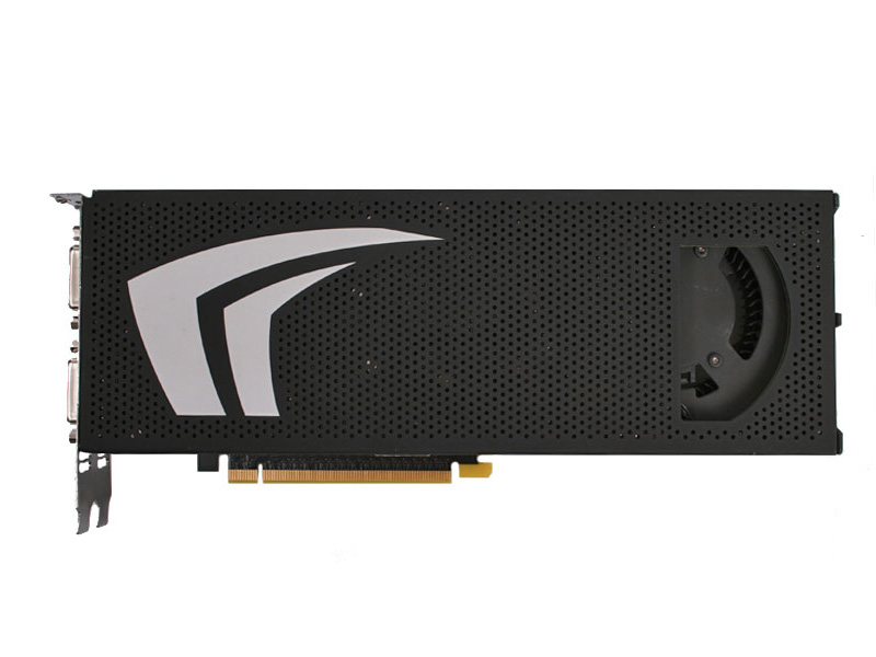
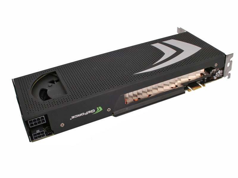
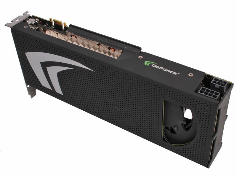
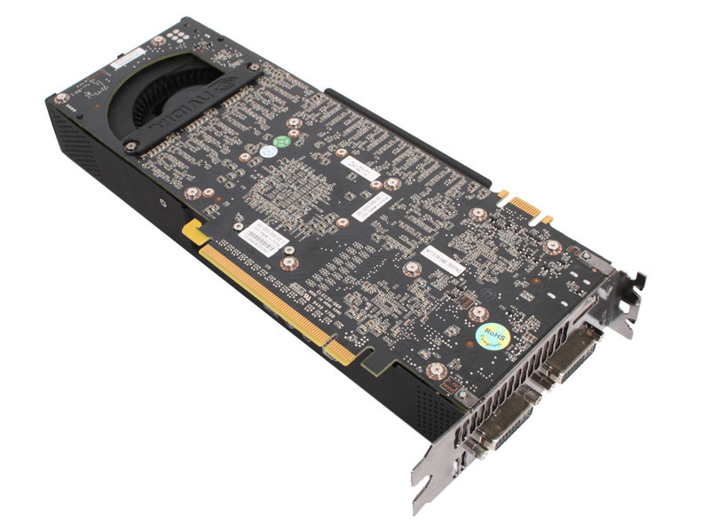
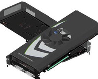
Click to enlarge
It combines a pair of 55nm GT200 chips on a single graphics card that's similar to the GeForce 9800 GX2 in design – it’s a dual PCB design that is the same length as the GeForce GTX 280 and has the cooling solution sandwiched between the two PCBs. There are the full 240 stream processors enabled on each of the GPUs, meaning 480 in total. These are clocked at 1,242MHz – the same speed as they are clocked on the GeForce GTX 260 (both revisions).
As the texture units are associated with each stream processing cluster, there is a full allocation of 80 per GPU, 10 per stream processing cluster and 160 in total. When combined with a 576MHz ‘core’ speed, this results in an impressive texture throughput of 92.2 GigaTexels per second.
Each chip backs out onto 28 ROPs (or render backends), making a total of 56 in total and, like previous GPUs derived from Nvidia’s G80 graphics processor, they run at the same speed as the texture units and setup engine. This means there is a 448-bit memory interface per GPU and Nvidia has kitted each GPU out with 896MB of memory (1,792MB in total) clocked at 1,998MHz effective.
What we’re looking at, then, is essentially a pair of GeForce GTX 260+ graphics cards in SLI, but with 240 stream processors per GPU instead of 216. This was something that confused us a little because, when we reviewed the GeForce GTX 260-216, we came to the conclusion that it was running out of memory bandwidth – there were many scenarios where the GeForce GTX 260-216 wasn’t discernibly faster than the original GeForce GTX 260.
Click to enlarge
When we asked Lars Weinand, Senior Technical Marketing Manager at Nvidia, why Nvidia had gone down this route, he said that it “needed to leave headroom for partners doing overclocked editions [of the GeForce GTX 295]. Our reference design spec is not a given law and partners do their own products with higher specs on the high end. They like to call that overclocked, but in the end it’s a higher spec’d variant.”
That’s fair enough, but we feel that an additional 200MHz (or so) on the memory clock would have helped the GeForce GTX 295 along the way. Even before testing, we were sure that there would be scenarios where the card would not release its full potential due to limited memory bandwidth because we saw exactly the same thing with the GeForce GTX 260-216.
The board design incorporates an improved heatsink, which Nvidia says is capable of dissipating more than 289 watts of power – which, incidentally, happens to be the maximum quoted board power for the GeForce GTX 295. This is a massive improvement over the GeForce 9800 GX2’s heatsink from our perspective as that particular design actually cooked certain SLI certified motherboards.
The design also does away with the shiny painted finish of the GTX 2xx family as well; instead, soft touch paint has been used for a matte look and feel. We like this, and it’s an evolution of the shiny design – the only thing we didn’t like about the old finish was how it attracted finger prints.
One thing that Nvidia hasn’t really fixed though is the placement of the power connectors – each PCB has its own power connector (one six, one eight) and they are opposite each other like they were on the 9800 GX2. Nvidia has removed the metal that surrounded them on the GX2 (and made it incredibly difficult to plug the cables in), but that’s not our issue. The issue is that they’re still directly opposite each other, which means removing them requires fingers thinner than a scalpel blade – can they not be slightly offset to make removal slightly easier?
RELATED ARTICLES


MSI MPG Velox 100R Chassis Review
October 14 2021 | 15:04

Want to comment? Please log in.