AMD has long had a reputation as the chip manufacturer of choice for gamers and enthusiasts. The Athlon 64 platform has been a massive winner for the firm, with performance to get excited about across a whole range of chips, from the cutting-edge FX-60, to more moderate chips like the X2 3800+.
Today, AMD is migrating its Athlon series to a new platform - AM2. This is a new CPU series and socket type. These new CPUs come with a memory controller on-chip, as the old ones did, but the major difference is that this controller is DDR2. Finally!
We have a couple of articles going up today, one documenting AMD's new platform and one documenting a new motherboard chipset from NVIDIA, the nForce 5. Over the coming days we'll also be bringing you a motherboard group test of the best Socket AM2 motherboards. In this article, however, we'll be looking at AMD's major new CPU releases today - The FX-62 and the 5000+.
In the meantime, on with the show!

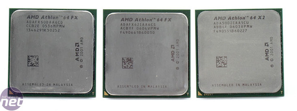
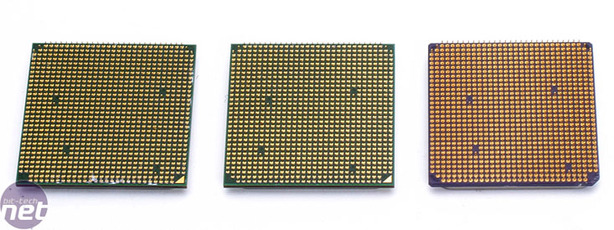
Athlon 64 FX-60 (939), Athlon 64 FX-62 (AM2), Athlon 64 X2 5000+ (AM2)From the top, there are no visible differences in the heatspreader design or the size of the packaging. The changes don't become apparent until you look at the pin layout on the bottom of the processor packaging. The first difference between Socket 939 and Socket AM2 is the extra pin in the bottom left hand corner of the AM2 chips, making a total of 940 pins.
This is just like the additional pin on the Socket 940 chips, too (pictured right). With that said, the pin layout is very similar to that of the older Socket 940. However, there are enough differences in the pin layout to make it impossible to install an AM2 chip in a Socket 940 board, and vice versa.

Socket 939, Socket AM2, Socket 940The right hand blanking areas (the areas without pins) on the back of both the Socket 939 and Socket AM2 chips are similar positions - both are on the same line of pins, with the blanking areas five pins and seven pins in from the right hand edge of the chip respectively. Socket 940 is a little different in that respect - the upper-most blanking area is seven pins in from the edge, while the bottom blanking area is in the same position as both Socket 939 and AM2.
The differences between the left hand blanking areas are quite different across all three socket designs, though. The lower blanking area has been moved two pins closer to the left edge edge, while the top blanking area has moved in the opposite direction. Instead of being five pins away from the edge (on Socket 939), it is now seven pins away.
We get the impression that there probably wasn't a need for AMD to actually make a socket change in order to add DDR2 memory support into its K8 architecture. We must remember that the memory controller is located on the CPU die and not in the north bridge. This means that there could be a slew of confusion over what components work with the new CPUs if the pin layouts were the same. In fact, that is probably the main reason for AMD choosing to change from Socket 939 to Socket AM2.
Looking at the situation from another perspective leads to the prospect of causing headaches for AMD's customers. Even if the CPU didn't require a pin layout change, the change enables AMD and its partners to control which components work with the new processors. In that respect, we think that it makes a lot of sense to make changes to the pin layout in order to prevent consumers installing one of the new AM2 processors into a motherboard that doesn't support DDR2 memory, or vice versa - installing an older CPU into one of the new motherboards supporting DDR2.
Today, AMD is migrating its Athlon series to a new platform - AM2. This is a new CPU series and socket type. These new CPUs come with a memory controller on-chip, as the old ones did, but the major difference is that this controller is DDR2. Finally!
We have a couple of articles going up today, one documenting AMD's new platform and one documenting a new motherboard chipset from NVIDIA, the nForce 5. Over the coming days we'll also be bringing you a motherboard group test of the best Socket AM2 motherboards. In this article, however, we'll be looking at AMD's major new CPU releases today - The FX-62 and the 5000+.
In the meantime, on with the show!
Physical Appearance:

Athlon 64 FX-60 (939), Athlon 64 FX-62 (AM2), Athlon 64 X2 5000+ (AM2)
This is just like the additional pin on the Socket 940 chips, too (pictured right). With that said, the pin layout is very similar to that of the older Socket 940. However, there are enough differences in the pin layout to make it impossible to install an AM2 chip in a Socket 940 board, and vice versa.

Socket 939, Socket AM2, Socket 940
The differences between the left hand blanking areas are quite different across all three socket designs, though. The lower blanking area has been moved two pins closer to the left edge edge, while the top blanking area has moved in the opposite direction. Instead of being five pins away from the edge (on Socket 939), it is now seven pins away.
We get the impression that there probably wasn't a need for AMD to actually make a socket change in order to add DDR2 memory support into its K8 architecture. We must remember that the memory controller is located on the CPU die and not in the north bridge. This means that there could be a slew of confusion over what components work with the new CPUs if the pin layouts were the same. In fact, that is probably the main reason for AMD choosing to change from Socket 939 to Socket AM2.
Looking at the situation from another perspective leads to the prospect of causing headaches for AMD's customers. Even if the CPU didn't require a pin layout change, the change enables AMD and its partners to control which components work with the new processors. In that respect, we think that it makes a lot of sense to make changes to the pin layout in order to prevent consumers installing one of the new AM2 processors into a motherboard that doesn't support DDR2 memory, or vice versa - installing an older CPU into one of the new motherboards supporting DDR2.

MSI MPG Velox 100R Chassis Review
October 14 2021 | 15:04


Want to comment? Please log in.