AMD Bulldozer Front-end
Increasing the pipeline length of a CPU is a reliable way to enable higher frequencies, but it brings risks. If your scheduler, pre-fetch unit and branch prediction algorithms aren’t up to the task you can get trapped in processing instructions in an inefficient order, or having the CPU pipeline stall due to not having the right data in the cache or pipeline. This is fine in a short pipeline, as the consequence of unpredicted branch merely means flushing a few instructions to cache, fetching the right data, flowing that down the few stages of pipeline that are now clear. With a long pipeline, that process takes ages, leading to long stalls; stall often and the processor spends most of its time idle.Famously, Intel learnt this the hard way – the prefetcher, branch prediction unit and scheduler had to be amazing to cope with the latter Pentium 4s that Intel was making. Intel is said to have taken those units and that knowledge and bolted them onto the more efficient (much shorter) execution core it borrowed from the Pentium Pro to make Conroe.
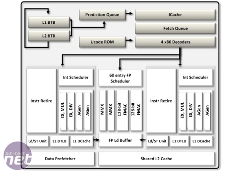
Back to Bulldozer, and AMD says it has designed the front end of a Module to suit the bursty nature of data flowing into a CPU, saying that you therefore don’t need a large front end (which will sit idle in between data bursts) but loads of execution power to handle large data bursts without queuing becoming an issue. Therefore, there’s one front-end unit shared between two execution cores in the Bulldozer design. Or, in AMDese, Bulldozer ’maximise[s] peak bandwidth across the different cores, and maximise[s] the use of silicon area through the use of shared modules.’
The savings in silicon area have been spent on ‘predition-directed instruction prefetchers… A Prediction Queue can manage direct and indirect branches that are now fed with a Level 1 and Level 2 Branch Target Buffer, and stores destination addresses. Bulldozer Modules can decode up to four instructions per cycle (versus three on AMD Phenom II processors.’ Essentially, the front-end is smarter and more capable than previous AMD front-ends, not only to prevent stalls in the longer pipeline, but to keep two execution cores fed with work as much as possible.
AMD has also implemented a physical register file (PRF) to act as a single repository for ‘register results of executed instructions.’ The reason given is that this ‘eliminates unnecessary data movement and data replication’ and also saves power by not needing to broadcast its contents to other registers.
Cache arrangement
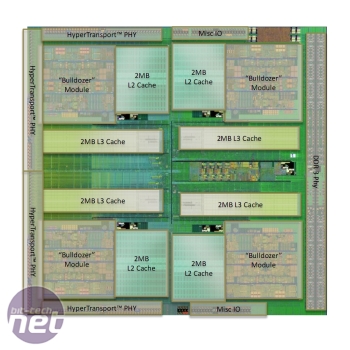
Each execution core has its own Level 1 cache, with 16KB for data and 64KB for instructions. This is a reduction compared to the 128KB per core of a Phenom II, but is compensated for by the 2MB of Level 2 cache inside each Module. A Phenom II core had 512KB to itself in most CPU models. Each Module is then connected to 2MB of Level 3 cache, though it’s worth noting that even 6- and 4-core Bulldozer CPUs retain 8MB of Level 3 cache despite having disabled Modules.AMD has also moved to an inclusive cache design, a move that Intel made with the Bloomfield-design Core i7-900 series in November 2008. Inclusive caches don’t seem to make sense at first, at it literally means that all of the lower-level cache is also saved in the higher-level, which initially looks like a waste of cache.
However, it means that the higher-level cache essentially acts as a snoop filter – if Core 1 needs data that Core 5 is working on, it can merely fetch the most current version from the Level 2 or Level 3 cache without the need to interrogate Core 5 and thus prevent it from processing the work its currently doing. Despite seeming wasteful, inclusive caches are more efficient for massively multi-core processors as they help to keep all the cores working more of the time.
Memory controller upgrades
As FX-series CPUs slot into Socket AM3+ motherboards, the memory controller is a dual-channel DDR3 unit that operates at a maximum official frequency of 1,866MHz. It can officially accept DDR3 rated at 1.5V or 1.65V, though motherboard makers are likely to implement DDR3L (low-power DDR3) voltages, as it’s a handy feature for saving power.
MSI MPG Velox 100R Chassis Review
October 14 2021 | 15:04




Want to comment? Please log in.