Enter Sand, Man
We’re pretty sure that most computer enthusiasts are aware that CPUs are made from silicon. Far fewer are likely to realize exactly how much work goes into making what is effectively a wonder of the modern world. Processors are made on a mind bogglingly small scale to withstand huge tolerances, with even the cheapest chips requiring hundreds of manufacturing stages to get from wafer to motherboard.Manufacturers are also under pressure to improve production methods and reduce transistor size, with different companies approaching the problem in different ways. Intel helped us put this guide together, and as a result it focuses on its implementation of the 32nm High-K manufacturing process. Other manufacturers, such as Global Foundries or TSMC, use subtly different methods to produce its chips.
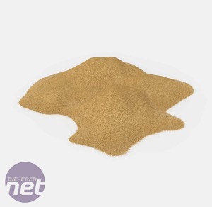
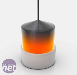
Left: Its got a long way to go from here. Right: It's important to make the silicon ingot a single, join-less piece.
Amazingly, after oxygen, silicon is the most plentiful element in the earth’s crust. It’s not just lying around in electronics-grade lumps though, and needs to be extracted from sand, where it resides in the form of silicon dioxide (SiO2).
Once the silicon has been purified to the required degree (something in the region of 99.9999999 per cent pure), it's formed into a single contiguous 100kg ingot of silicon. The ingot can then be sliced into individual 1mm thick disks, called wafers, which should be recognizable to most tech junkies.
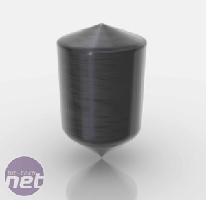
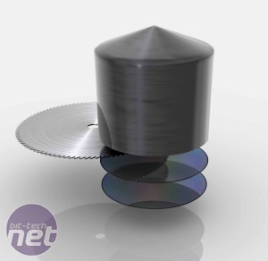
Left: These ingots weigh up to 100kg and are around 12 inches in diameter. Right: The wafers have to be precisely the right thickness.
The wafers are then polished to a flawless mirror finish ready for the next stage of the process. Interestingly, CPU manufacturers are not normally responsible for these initial stages, instead buying ready cut and polished wafers from third-party silicon producers.
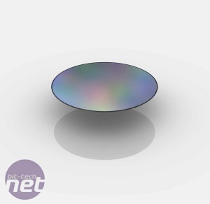
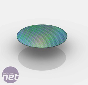
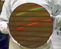
Left: The cut and polished silicon wafer all ready to be made into a few hundred processors. Right: You can just see the patterned sheen of the photo resist.
Now the complex business of creating something capable of playing Crysis and rendering video begins in earnest. The wafer is covered in a strategically pattered layer of photo resist, which acts like a stencil for when the wafer is bombarded with high powered beams of charged atoms called ions.
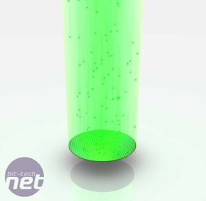
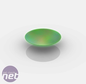
Left: Beam me up Scotty... or just embed me with trillions of charged ions. Right: The electrical conductivity of certain parts of the wafer has now been changed.
The ions embed themselves in the exposed parts of the silicon, in a process called ion implantation or doping, leading to a change in the conductive properties of that part of the wafer. The photo resist is then removed, leaving behind a complex pattern of conductive and non conductive traces on the silicon wafer.

MSI MPG Velox 100R Chassis Review
October 14 2021 | 15:04




Want to comment? Please log in.