
Intel Core i7 - Nehalem Architecture Dive
Manufacturer: IntelEvery so often in this industry someone says something that makes you do that funny double-take prompting you to ask that question of doubt: "I'm sorry, could you repeat that please?"
This happened when Intel first talked about Nehalem in some detail (as opposed to just announcing the name) - that was about six months before Penryn, Intel's first 45nm processor, made its way onto the market.
At that time, Intel revealed that its new Nehalem architecture would have an on-die memory controller, sparking the end to its institutional Front Side Bus model. It was a defining moment in the future of Intel's CPU microarchitecture, just like it was when AMD reinvented itself as a serious and, in some places, market leading manufacturer with the excellent K8 architecture and its integrated memory controller.
Some interpretations argue that Intel is admitting AMD was right to move the northbridge onto the CPU die in order to make things more efficient and that Intel’s very antiquated front side bus model was very quickly running out of steam. While the latter maybe true, Intel will no doubt argue that waiting until now was the right idea: with its 45nm process it can achieve a specific power density that offers acceptable performance and keeps costs reasonable. All of which could mean that despite being "late" with the technology, it could now develop an advantage.
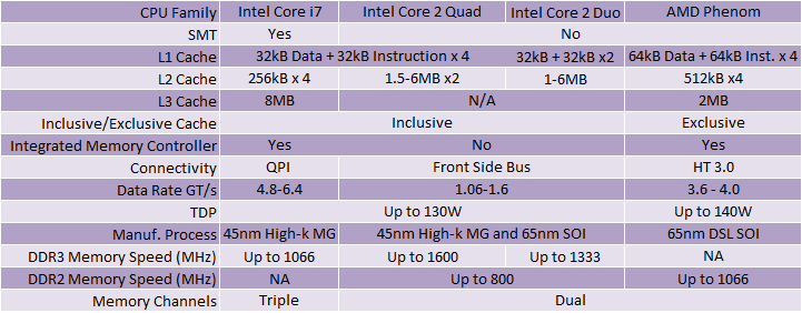
After the nightmare of Netburst, Intel designed the Core microarchitecture with top to bottom scalability of utmost importance – right from multi-socket server down to ultra-portable notebooks. That’s an incredibly difficult task – to balance power saving that’s most important in battery limited mobile applications, to highly scalable, ultra high performance servers.
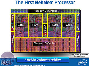
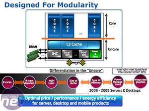
This is where Intel's "modular" design comes in – even though Nehalem is a bigger, more complex die, internally it's split into parts that can in theory be mix and matched like simple building blocks.
If you need more cores, or integrated graphics, or more QPI links; just drop them in. Intel splits the CPU into the Core(s) section and Uncore section that has, well, everything else. AMD has also cited itself to take this approach when we first heard about its next generation Fusion CPU - so by both retaining an element of flexibility it can approach and satisfy new markets quicker and meet the competition sooner, both of which are good for us as consumers.
While on some level Nehalem was designed with this in mind again, in others this greater diversity in product type will also bring many more new sockets than we’re currently used to. This diversity will focus the greater populous of its users into particular hardware models that will be optimal products for their needs, however it could also mean upgrading costs far more if you decide to jump between boundaries - it's not just a CPU, it's the motherboard and possibly memory as well.
It will also be the death of extreme value overclocking – will we get another Celeron 400a, Celeron DP (Abit BP6), 1.0 Athlon AXIA/AVIA Thunderbird, Northwood 1.6a, Core 2 Duo E5200 or Core 2 Quad Q6600? Bargain CPUs that act like Extreme Editions 10x their price when overclocked, and while bad business for Intel, fantastic for enthusiasts on a budget.
The new Core i7 brand was recently revealed as the official naming of Nehalem. We've also since been told that the "7" portion doesn't particularly mean much, although we expect there will be Core i5/6/8 etc as future processor sockets with specific abilities get introduced next year.
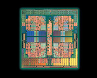
- Die size - Nehalem has a larger 263mm² versus 214mm² for Yorkfield (both cores included)
Transistor Count - Nehalem's is actually lower at 731M versus 820M for Yorkfield, this is mostly because of the reduction of overall cache: 9MB L2 and L3 versus 12MB L2, as SRAM cells require four transistors per bit.
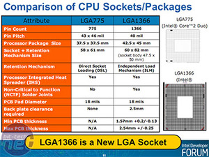
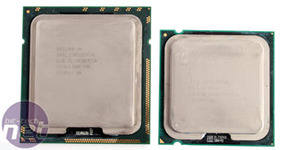
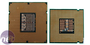
Physical Size - LGA1366 is considerably larger at 45x42mm versus 37x37mm for LGA775.

MSI MPG Velox 100R Chassis Review
October 14 2021 | 15:04



Want to comment? Please log in.