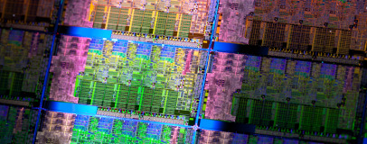
What's New in Intel's Sandy Bridge
Intel has beaten AMD to be the first CPU company to integrate a GPU into the silicon die of an x86 processor – it managed to integrate a GPU into the processor packaging for its Clarksfield-based Core i3 and Core i5 CPUs. We expect AMD’s Fusion combined CPU-GPU chips early this year, with desktop parts available in mid-2011.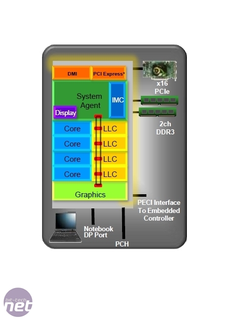
Sandy Bridge uses a ring bus to connect its sub-units.
The interesting aspect regarding the graphics unit is that it shares the ‘last-level’ cache (LLC) of the entire die with the CPU execution cores. Intel’s Shared Cache technology has worked incredibly well for it over the years.
There’s a big pool of Level 2 or 3 cache, and any CPU can reserve any amount it requires, therefore making that cache work as efficiently as possible. Allowing the GPU to tap into this shared resource is a logical step, but it required a radical rethink of how processing units access and address it.
In the end, Intel has implemented a ring bus, and not even an Intel Ring Bus Technology®, which is an odd move for a company that loves to brand anything and everything that it creates.
A ring bus controller polls each unit in a looping sequence, accepting or offloading data as it progresses – if the GPU requires data from the main memory (via the processor cache), it will have to wait until the CPU cores have been served first, before sending that request to the System Agent unit, which can pass it onto the integrated memory controller.
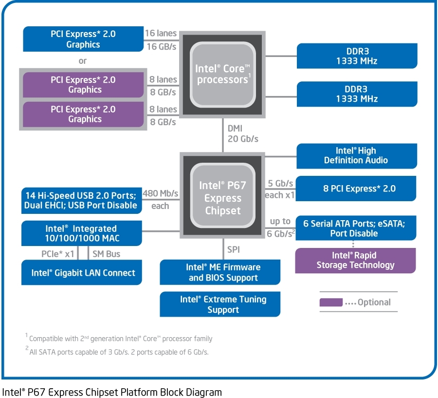
The layout of a P67 motherboard: you'll
need one of these to overclock a Sandy Bridge CPU.
Click to enlarge.
This may not sound significant, but it means that overclocking via the Base Clock is extremely limited, if not impossible, as even sensitive buses such as SATA are linked to the ring bus clock.
In our testing, we found that increasing the Base Clock beyond 105MHz (from the default 100MHz) resulted in lock-ups and crashes no matter which other BIOS options we tried.
Overclocking is possible with Sandy Bridge CPUs, however – there are details throughout this article, and we gather all the overclocking settings for all the CPUs we've tested (and re-tested) on the How to Overclock an LGA1155 CPU page. We'll bring you a more in-depth overclocking article soon.
RELATED ARTICLES


MSI MPG Velox 100R Chassis Review
October 14 2021 | 15:04

Want to comment? Please log in.