
Introducing Penryn
The Penryn family is an enhanced derivative of the incredibly successful Core microarchitecture, with most of the same design principles used and some tweaks made. Wolfdale, the desktop version of the Penryn family of CPUs, is a die shrink of Conroe and like the chip it’ll be replacing, Wolfdale is still a native dual-core processor.Because of this fact, the quad-core derivative of Wolfdale, Yorkfield – the processor which we’re looking at here today, is exactly the same as what Kentsfield was in relation to Conroe. It is merely a pair of Wolfdales on the same silicon substrate package and thus fits into a single LGA775 socket.
Theoretically, shrinking a 65-nanometre design to 45-nanometres would result in a die that’s less than half the size. For comparative purposes, the Conroe die was a 291-million transistor design with a surface area of 143mm² whereas the Wolfdale die is 410-million transistors on a 107mm² die. If Wolfdale was Conroe on a bitterly cold winter day, its surface area would be somewhere around the 70mm² mark – at least, that would be the theory.
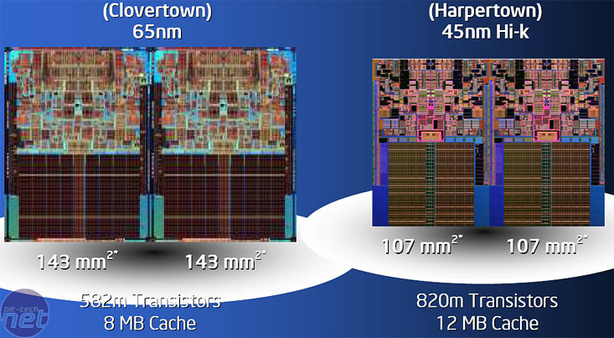
Clovertown and Harpertown are the server equivalents to Kentsfield and Wolfdale
In reality though, Wolfdale isn’t just Conroe out in the cold; it is a 410-million transistor behemoth, which equates to around a 40 percent increase in transistors over Conroe. This increase is attributed to the increased L2 cache of 4MB to 6MB, as well as some new features that contribute to some of the difference. Despite the increased transistor count, Wolfdale’s die is 33 percent smaller than Conroe’s, which is all thanks to the improved manufacturing process.
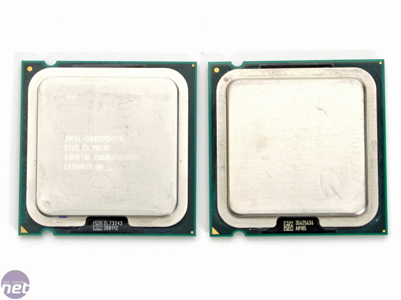
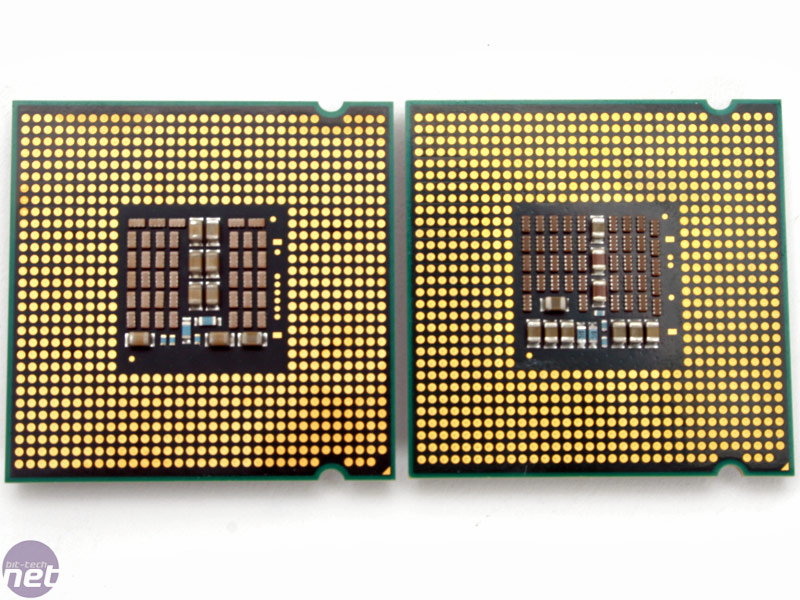
New Yorkfield on the left and old Kentsfield on the right
When Intel unleashed the Core microarchitecture, it was clear to point out that there were five key components in the design – Wide Dynamic Execution, Advanced Smart Cache, Smart Memory Access, Advanced Digital Media Boost and Intelligent Power Capability – and they each contributed to the design in several ways. The philosophy was very much focused around performance-per-clock and performance-per-watt unlike the days of Netburst where the focus was just sheer clock speed and throughput – keeping everything as active as possible.
Penryn is no exception to the new design philosophy and makes some improvements on the original Core microarchitecture. Probably the easiest way to discuss the changes and enhancements made in the Penryn family is to go back to our initial look at Intel’s Core 2 Duo processors, where we outlined the five key components that make up the Core microarchitecture. Over the page we'll describe the enhancements Intel has made to the architecture.
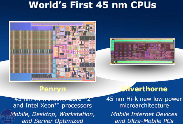
Before we do that though, it's worth briefly mentioning Intel's other 45nm architecture – Silverthorne. It is the first dedicated mobile processor from Intel that is a fraction of the size of normal CPUs and is specifically tailored for low power devices. When the Tejas and Jayhawk project was cancelled back in 2005, the architect team was split into two groups: the first was tasked with designing Penryn architecture while the second designed Silverthorne.
Despite working on two completely different architectures, both had one common goal: working exclusively towards the anticipated 45nm manufacturing process, though they're using the process differently. As the increase in transistor switching speed and reduced current leakage are non-simultaneous benefits, the mobile parts sacrifice transistor switching speed for power reduction and battery life, whereas the desktop and server parts are more focused on performance as they have a much higher acceptable power envelope.
The difficulty in working with projected guidelines before a process is properly developed is fully evident with Tejas - the 90nm process was not what it was cracked up to be and so the CPUs leaked like a sponge and were said to be 150W at just 2.8GHz. In complete contrast, the 45nm process seems to have worked as anticipated or better than expected, as the launch has been brought forward slightly from initial projections.
RELATED ARTICLES


MSI MPG Velox 100R Chassis Review
October 14 2021 | 15:04

Want to comment? Please log in.