NVIDIA nForce 680i LT SLI
The almost non-existent nForce 590 SLI Intel Edition chipset meant that the nForce 680i SLI chipset was brought forward into late last year. With the overwhelming popularity of Nvidia’s SLI platform, the problem that the company has encountered is that its flagship chipset is too expensive and it alienated a lot of enthusiasts with a £180-plus price point. At the other end of the scale, nForce 650i SLI boards are available for as little as £80, but these boards come with only a fraction of the feature set you’ll get on a 680i board.The massive difference in price has lead to other chipsets like Intel’s P965 filling the void, or companies like Asus manufacturing boards with unofficial hybrid chipset combinations based around the cheaper nForce 650i SLI northbridge and more feature filled nForce 680i SLI southbridge.
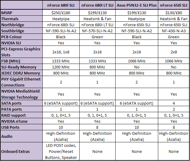
To fill this market gap, Nvidia has launched its nForce 680i LT SLI chipset, offering features and price somewhere in between the other two chipsets.
Feature List

All of the more useful features have been kept, including the six SATA 3Gbps ports and 1333MHz FSB strap to support the upcoming E6x50 Core 2 Duo processors. Nvidia has docked two USB 2.0 ports, but there are still eight available. How many people actually use all ten USB 2.0 ports concurrently? In that respect, who actually uses both Gigabit Ethernet sockets? And how about on board power and reset switches or POST LEDs – are they really necessary?
Of course, they are great for people like ourselves who mainly use motherboards flat on a test bench, but it will only be the rare occasion that an end-user really needs them. By not having to pay for things you don’t use, the necessary features are included and value for money is increased.
Despite the fact that Nvidia states that the overclocking is less likely to live up to nForce 680i SLI standards, the chipset is a completely refurbished microstructure which some manufacturers have told us can promote better overclocking than it's bigger 680i SLI brother. One went as far as to tell us that nForce 680i LT SLI had been reprogrammed to get rid of the "errors" that were present in the initial nForce 680i SLI. Since Nvidia wouldn't confirm these allegations, we don't know whether this is true or not.
The loss of SLI Ready memory up to 1200MHz isn’t a huge deal either, as there is still oodles of performance available with low latency 800MHz SLI ready memory. When overclocking, setting the memory to a 1:1 sync enables maximum front side bus increases, and thus huge memory speeds aren't wholly necessary.
From a software perspective you still get Nvidia’s Windows BIOS updater and nTune software. The latter allows you to adjust BIOS settings while you’re inside your operating system. In addition, there is the same Drive Management, RAID and Ethernet software like MediaShield and FirstPacket technologies that came with the standard nForce 680i SLI motherboards.
Just like the original nForce 680i SLI, Nvidia stresses that the reference boards are engineered for overclocking, with six-layer PCBs, overspecified voltage regulators and additional heatsinks where necessary. This isn’t to say we haven’t seen this from other companies previously, but it’s nice to have it reaffirmed from a chipset manufacturer and motherboard maker.
The EVGA nForce 680i LT SLI motherboard is built around the reference design and despite the change of PCB colour it’s simply a case of component removal from the original 680i reference design. It’s true that many enthusiasts, including ourselves, have had trouble with early batches of the reference EVGA nForce 680i SLI motherboard, but it seems Nvidia has learnt from its manufacturing mistakes as we’ve not heard the same story this time around.
As far as power requirements go, nothing has really changed from the original nForce 680i SLI: Nvidia still recommends SLI certified power supplies of 500-600W on high end systems. Specifically, they must have a +12V line with at least 30A total and 22A dedicated for the motherboard, 11A of which is to be dedicated for graphics use and 5.5A supplied to two six-pin auxiliary graphics power connectors.

MSI MPG Velox 100R Chassis Review
October 14 2021 | 15:04


Want to comment? Please log in.