Under the heatsink
Taking things apart is something that every self-respecting geek should do, regardless of how expensive or how precious the item is – it’s all about broadening the mind here. As such, it’s almost a ritual now at bit-tech for us to strip today’s (and tomorrow’s) latest and greatest hardware down to its bones.Unlike the GeForce 9800 GX2, taking apart the Radeon HD 4870 X2 wasn’t the first thing we did when we got the hardware – time was much more valuable this time around, and the last thing we wanted to do was end up with a dead card just a few days before the launch. Now that wouldn’t have been cool.
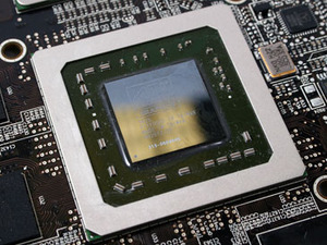
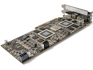
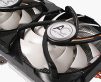
The first thing we noticed was that both of the heatsinks cooling the GPUs were copper – that’s unlike the Radeon HD 3870 X2, which had one copper and one aluminium heatsink under the shroud. I guess the increased heat output on RV770 was enough to mean that an aluminium heatsink was no longer up to the task.
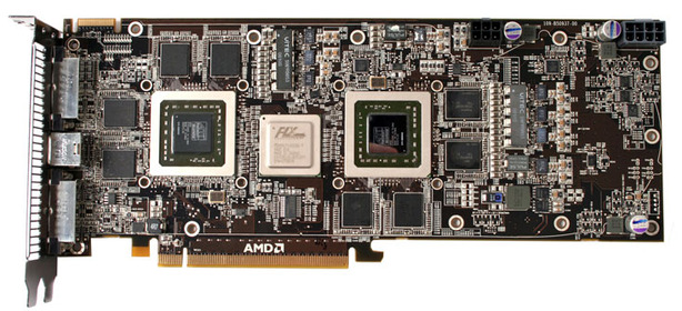
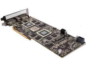
Layout-wise, the 4870 X2's board looks incredibly similar to the card it's replacing although again there are quite a few changes that become apparent upon closer inspection. First of all, there are 16 128MB Hynix 4.0 Gbps GDDR5 DRAM chips on the board—eight per GPU—meaning there’s a total of 2,048MB of memory on the card. However, because the card uses CrossFire technology and memory isn’t shared between the two RV770 GPUs, each ASIC has access to 1,024MB of local memory and the contents are duplicated across both pools.
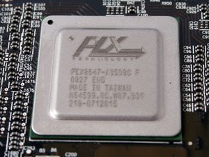
The bridge chip’s appearance and size have also changed – the PLX Technology PEX8647 switch delivers features 48 lanes (split three ways) of PCI-Express 2.0 connectivity. Each GPU is connected to one of the three x16 lanes, while the remaining x16 lane is the interface between the graphics card interconnect and the motherboard’s PCI-Express bus.
We’ve already mentioned that the PEX8647 supports broadcasting data to both GPUs simultaneously (coined Dual Cast by PLX), but upon looking through the chip’s datasheet, we learned that it also supports a technology called Read Pacing. What this does is it allows the number of read requests to be throttled to any one of the three ports in situations where other ports may become starved because the read request queue for one port is taking longer than expected to chew through, and is therefore having a negative impact on performance. With Read Pacing, the read requests that are taking longer than expected should be better scheduled to hide potential performance dips.
The other thing worthy of note is the number of power phases on the card. Each GPU appears to have three power phases with an additional phase for each 1,024MB memory pool. Again, this has changed from the HD 3870 X2’s PCB, which had just two power phases per GPU – it’s another clear sign that RV770 isn’t as frugal as RV670 when it comes to power.

MSI MPG Velox 100R Chassis Review
October 14 2021 | 15:04





Want to comment? Please log in.