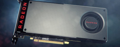
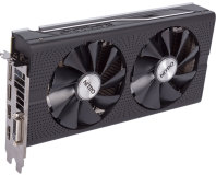
The Polaris Architecture
The most impactful change with Polaris is the move to the Samsung/Global Foundries 14nm FinFET process. Polaris 10 crams 5.7 billion transistors into an area of just 232mm2, which makes the 28nm parts seem massive in comparison: the R9 390X, for example, has a few extra transistors (6.2 billion) but a far bigger die size of 438mm2. The transition is also responsible for the reduction in power consumption and increase in clock speeds, with the FinFET transistors having lower operating voltages and reduced leakage, helping to improve efficiency. As a 150W part, the RX 480 is ripe for small form factor cooling solutions.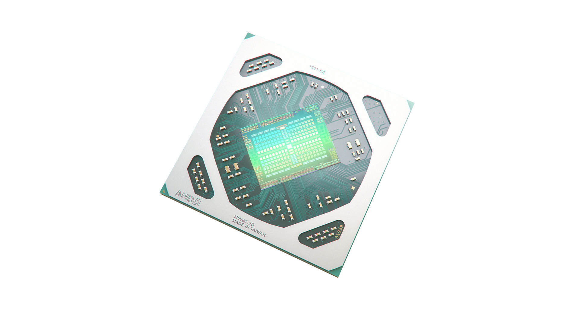
Click to enlarge
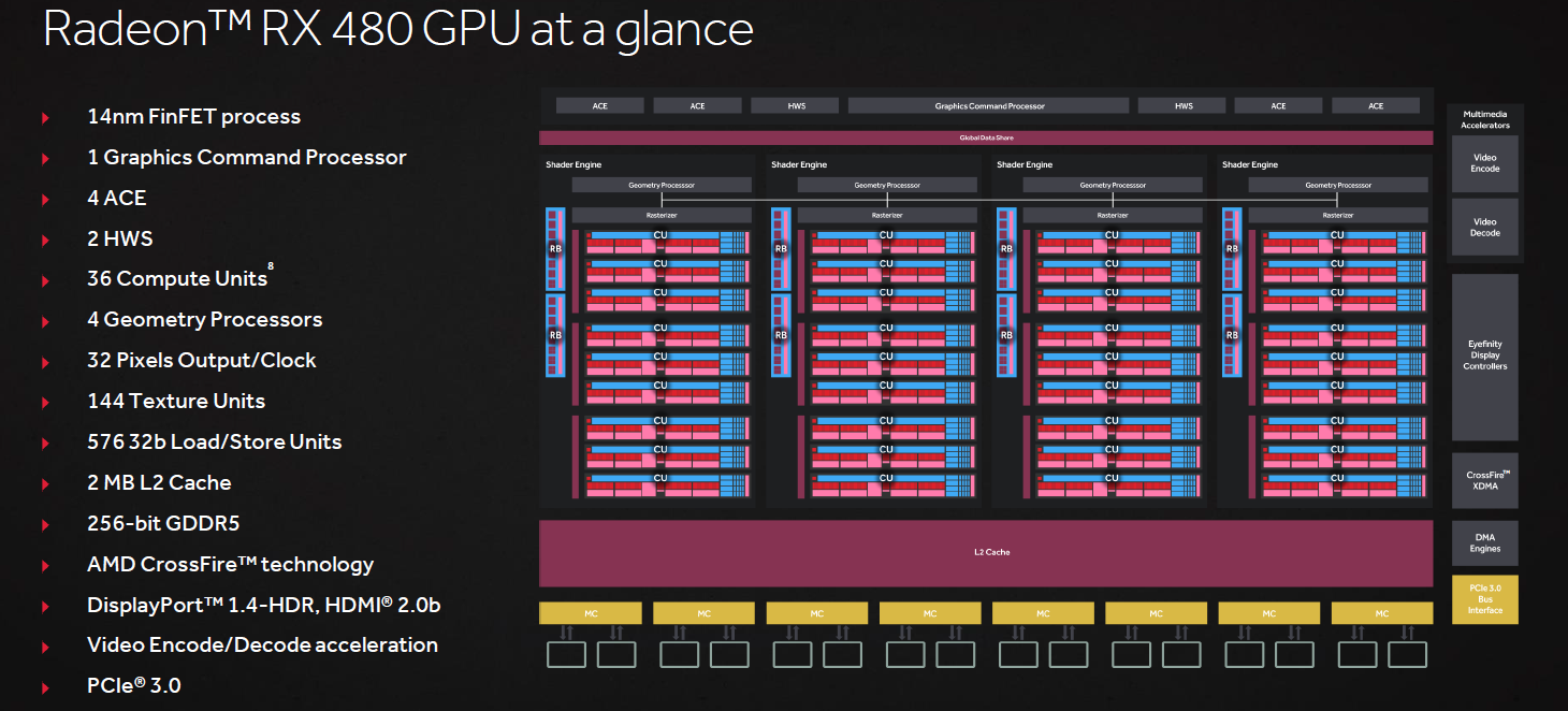
The high level block diagram is a largely familiar picture. Dishing out work at the front-end is the Graphics Command Processor joined by four Asynchronous Compute Engines and two Hardware Schedulers. The bulk of the processing is done by the four Shader Engines, each with its own geometry processor, rasteriser, nine Compute Units and two Render Back-End Units. With 64 cores and four texture units per CU, we're left with totals of 2,304 and 144 respectively, and the eight Render Back-End Units net us 32 ROPs. The Shader Engines share the L2 cache, and all that's left then are the usual memory controllers and hardware blocks for video encode/decode, Eyefinity and CrossFire. This is the Polaris 10 GPU in its fullest configuration – the RX 480 doesn't have any parts disabled.
Click to enlarge
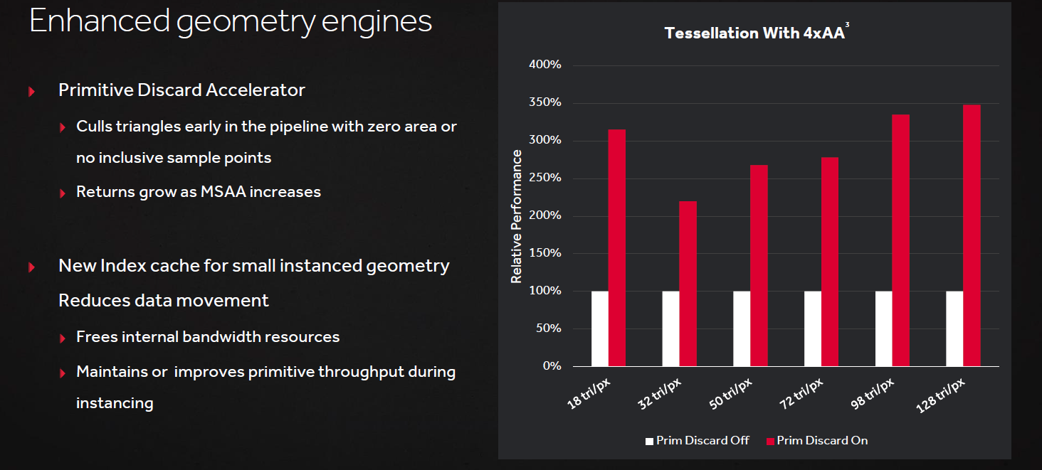
Geometry processing is one area AMD has focussed on improving. Each of the geometry engines has been given a primitive discard accelerator. This is designed to calculate early on in the pipeline which areas of geometry in a given frame will not actually be visible to the user and thus which do not need to be rendered, thus preventing unnecessary work. AMD has also added an index cache for instanced geometry, which is where areas of a scene that look alike (e.g. foliage or distant buildings) are copied instead of being needlessly rendered. The cache improves processing of this nature, freeing up resources for other work.
Click to enlarge
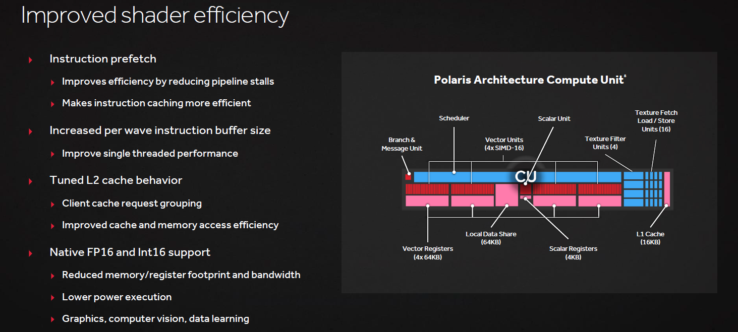
The Compute Unit, which is the backbone of the GCN architecture, remains unchanged in structure or in the size of its caches. Nonetheless, AMD has been able to improve shader efficiency with a few small tweaks. For example, better prefetch algorithms help to keep the caches filled with instructions for the cores to work on, thus keeping them busier and reducing stalls. Ultimately, AMD claims it has achieved up to 15 percent more performance per CU with GCN 1.4 – not revolutionary, but appreciated nonetheless.
Compared to the R9 290X, L2 cache size here has doubled to 2MB; the same as the Fury X, making it pretty big for a chip this size. We're also told that the way the L2 cache is utilised has been bettered. While this doubling is a sacrifice in terms of transistors and die size, AMD is able to keep more data on die as a result and reduce the need for comparatively slow and power hungry requests to external memory.

Click to enlarge
Where AMD loses die space in increasing the L2 cache, it gains it by halving its 512-bit memory interface to 256-bit, thus reducing the memory controller footprint. However, it still has to keep the cores fed, so it has had to maximise what it can do with this interface. Part of this comes from the L2 cache improvements, but another element is raw speed: AMD has enhanced the memory controllers to support the fastest GDDR5 speeds, hence the use of 7Gbps and 8Gbps memory in the RX 480.

Click to enlarge
The lossless delta colour compression engine has also been upgraded so that more frame data can be compressed and the available bandwidth is more efficiently utilised than before. AMD claims that performance per bit is up, on average, by 1.4x, which means that at 7-8Gbps (224-256GB/sec), the RX 480 is able to operate with similar or even more performance relative to Hawaii cards (320GB/sec), all while the memory interface consumes significantly less power – up to 58 percent less, according to AMD. Ultimately, we're assured that the RX 480 GPU won't be starved of memory bandwidth thanks to these improvements.
Further power efficiency gains have been made in Polaris with changes to the adaptive clocking algorithms and improved usage of sensors across the ASIC to reduce the GPU's operating voltage at a given frequency level, as well as a few other minor tweaks. The figures AMD wants you to take home are up to 1.7x performance per watt gains from the shift to the 14nm FinFET process along, and up to a 2.8x improvement in total once AMD's own optimisations are accounted for.
Click to enlarge
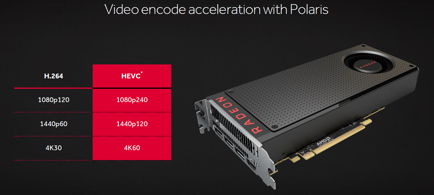
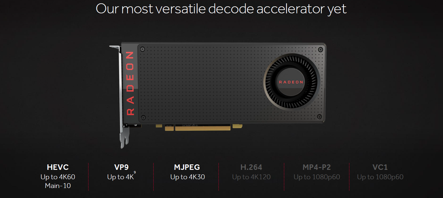
Lastly, it's worth mentioning the hardware video encode and decode capabilities. Polaris now supports HEVC encode up to 4K60, effectively doubling the capabilities of Fury X's H.264 support. New HEVC, MJPEG and VP9 capabilities have also been added to the decode accelerator, albeit with the latter planned for a future driver release.
RELATED ARTICLES


MSI MPG Velox 100R Chassis Review
October 14 2021 | 15:04

Want to comment? Please log in.