
Memory and ROP Architecture
With RV770, AMD made some big changes at the bottom end of the chip’s pipeline – not only did the company ‘fix’ the problems with its render backends (or ROPs), but the memory controller has also been completely redesigned.Part of this is because of the way the cache hierarchy has changed, but the rest of it is down to the fact that AMD felt it could achieve better bandwidth utilisation and a higher bang for buck when it came to transistor counts. It was no secret that the R600’s memory controller made up a significant amount of the total transistor count (and die space) – the same was true with RV670 as well.
When it came to working on RV770, AMD’s memory architects decided that a crossbar design was the way forwards. We’ve already talked about the cache hierarchy to some extent, whereby each SIMD has its own dedicated texture units and L1 texture cache – this is very different from the completely decoupled texture unit design used in the Radeon HD 2000/3000 series architectures.
Each of these texture caches is connected to a memory crossbar (or hub) and then data is allocated dynamically across the four memory controllers in a tiling method in order to maintain good locality of reference.
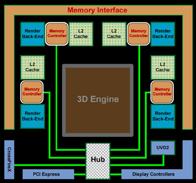 The four memory controllers are each associated with a ROP unit and an L2 cache—the main bandwidth consumers inside the chip—in a similar way to Nvidia’s recent designs. There’s no doubt that AMD has learned a few lessons from Nvidia’s G80 architecture in particular.
In addition, the hub is connected directly to lower-bandwidth interfaces like PCI-Express, the display controllers, the UVD video engine and the CrossFireX interconnect – this, AMD says, helps to improve overall bandwidth efficiency by around 10 percent compared to RV670.
The ROP or render backend units have been redesigned too and they’re now more powerful than those in the Radeon HD 3000-series cards. There are still only four of them, but they’re up to twice as fast as RV670’s units with multi-sample anti-aliasing enabled and even in 64-bit colour modes when AA is disabled. AMD says you’ll also see double the performance with Z-only operations too, with up to 64 ops per clock.
Having said all of that, I suspect that the peak throughputs for RV670 were a little optimistic because a lot of the problems with AA performance on the previous generation hardware were down to the fact there was no hardware-based MSAA resolve. Instead, MSAA resolve was done using the shaders and it was, err, rather slow. At this point, it’s worth mentioning that AMD’s custom AA filters will still use a shader-based resolve, but all of the conventional AA modes will use dedicated hardware in the render backends.
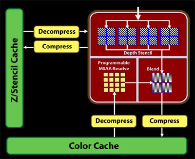
An RV770 render backend unit
Because of this, AMD worked with Hynix, Qimonda and Samsung to develop GDDR5 – a new memory type that uses a selection of techniques to achieve much higher bandwidth. These techniques include a new clocking architecture (with a quarter data-rate command clock), better error detection protocols, a new data mask algorithm and DRAM supported interface training.
When all of this comes together, the actual performance is actually four times the base clock. In the case of the Radeon HD 4870 the base clock is just 900MHz, but that’s quad-pumped meaning the effective clock rate is 3.6GHz, while data is humming along at a healthy 115GB/sec – and that’s all from a 256-bit memory bus, which makes for pretty impressive reading (and performance, too).
At the high-end, there's no contest in this particular test - the 4870 X2 smacks everything else around the chops quite literally. Meanwhile, the 4870 and 4850 seem to line up well against their competition. What's interesting though is that this test appears to be a little bandwidth limited, because there's quite a significant performance gap between the two RV770-based cards - much more than the core clock speeds and theoretical rates would have you believe.
RELATED ARTICLES


MSI MPG Velox 100R Chassis Review
October 14 2021 | 15:04

Want to comment? Please log in.