Texture Sampling
With RV770, AMD made some big changes to its cache hierarchy and texture sampling architecture. Those are very much still apparent in Cypress, but there have been some tweaks made in the general architectural upscaling.I mentioned earlier that there are 80 texture units across the entire Cypress GPU in its full fat form, but that only covers the chip's texture address capabilities. As a result, there's another way to look at the texture units when you take all of their capabilities into account and to save confusion, I've used slightly different terminology.
Each core has a texture sampler, which can handle four addresses, 16 FP32 samples and four FP32 filters per clock.
When everything is added up, the chip can now fetch 320 32-bit textures per clock (a rate of 272 billion 32-bit texture fetches per second) and bilinear filter 80 textures per clock (68 billion texels per second).
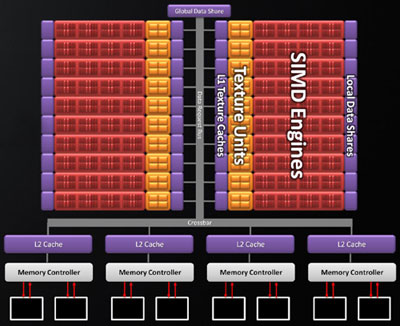
Cypress's texture cache hierarchy
The L1 texture cache has remained unchanged in terms of size and associativity - it still has effectively unlimited access per clock cycle - but the increased core count means that the number of texture caches has doubled. There are now twenty 8KB L1 texture caches, meaning a total of 160KB L1 texture cache GPU-wide. The four L2 caches, which are associated with each of the four memory controllers, have doubled in capacity as well and are now 128KB each, meaning a total of 512KB across the GPU.
Texture bandwidth has also been bolstered, with texture fetches from L1 cache happening at up to 1TB/sec (one terabyte per second) - that's more than double the L1 texture cache bandwidth available in RV770. I said so earlier, but it's worth reiterating again - that's a phenomenal amount of bandwidth. What's more, bandwidth between L1 and L2 caches has been increased to 435GB/sec from 384GB/sec on RV770 - another impressive figure.
See previous page for test kit
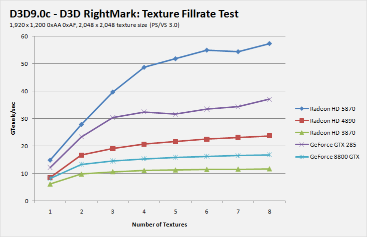
While 3DMark Vantage incorrectly reports the actual throughput, it appears to scale correctly compared to the other texture filtering tests we've done; the graph shows the relative performance across the various GPU architecture generations using a DX10 texture format. Our 3DMark06 multi-texturing test shows that the HD 5870 manages to get very close to its theoretical peak texture sampling rate, despite the massive amount of texturing horsepower available.
This is unlike RV770/790, which didn't get to 80 per cent of its theoretical peak throughput and is more in line with what we've come to expect from Nvidia's hardware. It's likely thanks to the hugely improved bandwidth to the L1 texture cache - D3D RightMark's texture fillrate test effectively confirms this.

MSI MPG Velox 100R Chassis Review
October 14 2021 | 15:04




Want to comment? Please log in.