ATI Cypress (RV870) Architecture
Cypress has been manufactured by TSMC on its 40nm process, and packs a breathtaking 2.15 billion transistors into its 334mm² die. The die brings back memories of the ill-fated R600 chip, as it's rotated by 45 degrees on its packaging.At 334mm², Cypress is a fairly mid-sized high-end GPU in the grand scheme of things, but it's not as small as AMD's 55nm RV770 (Radeon HD 4870) chip, which packed 956 million transistors into a surface area of 256mm². By comparison, Nvidia's GT200 chip was 576mm² on TSMC's 65nm process, while the 55nm GT200b die shrink reduced that to below 500mm². Both Nvidia chips featured approximately 1.4 billion transistors.
Die size is an important consideration for hardware vendors, because it has a heavy influence on manufacturing costs and margins. It's less of a concern for gamers, who really just care about a combination of performance, image quality, power consumption, heat and noise. The 300mm wafers on which the dies are manufactured have a fixed cost, but the number of dies per wafer increases or reduces costs accordingly.

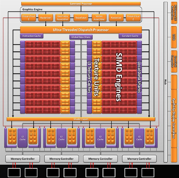
ATI Cypress architecture flow diagram
The Cypress architecture is very similar to AMD's previous unified shader architecture, so if you're familiar with R600, RV670 or RV770, you'll understand Cypress's origins. It's based on the VLIW (Very Long Instruction Word) philosophy introduced with the 2900 XT, but with the refinements and improvements added in RV770. There are more refinements with Cypress, and we'll run through them over the next few pages.
AMD has changed some of its terminology with Cypress because of the blurring lines between CPUs and GPUs. The stream processors have been renamed stream 'cores', but we haven't been wholly comfortable with AMD's terminology since R600, as not all of the stream processors (or stream cores as they're now called) are equal. Nvidia is just as bad as AMD in this respect, as it now refers to its stream processors as just ‘cores’.
A core isn't an execution unit though, as today's multi-core CPUs have multiple execution units per core - a core should be determined by its ability to fetch instructions from the instruction dispatch. This would still give RV770 and GT200 ten execution cores each, as both designs have ten stream processor clusters. This is still a strong marketing claim as well as being more accurate, even if a CPU core is still more complex and more flexible than those of a GPU.
In its full form, Cypress packs 20 SIMD units (or ‘cores’, given our definition above) with 16 five-way thread processors apiece, making a total of 1,600 stream processors. As with RV770, there are four texture units per SIMD, meaning the total number has doubled to 80 in Cypress. The number of render back ends (ROPs) has also doubled over RV770, meaning there are now 32. The memory bus remains unchanged at 256-bits, despite rumours to the contrary.
The ATI Radeon HD 5850, which we won't be discussing in great detail here, has 18 SIMD units (cores, by our definition) giving a total of 1,440 ALUs (stream processors in previous parlance) and 72 texture units.
The HD 5850 is clocked at 725MHz compared to the HD 5870's 850MHz engine clock, which reduces theoretical peak compute throughput from 2.72 teraFLOPS to 2.09 teraFLOPS. The HD 5850 keeps the 32 ROPs and 256-bit memory interface though, and, unlike the HD 4850, uses GDDR5 memory too. This is clocked lower at 1GHz (4GHz effective), compared to the 1.2GHz (4.8GHz) clock on the 5870, but that's still more than twice as much memory bandwidth as the HD 4850, and 11 per cent more memory bandwidth than the 4870 had.

MSI MPG Velox 100R Chassis Review
October 14 2021 | 15:04


Want to comment? Please log in.