ATI Cypress Shader Core
In terms of layout, Cypress's cores haven't changed a great deal compared to RV770 - there are just twice as many of them. Each core is still based on the idea of SIMD – Single Instruction, Multiple Data - and features 16 VLIW (Very Long Instruction Word) five-way superscalar thread processors. This is why ATI can claim to have 1,600 stream processors in total in the RV870, as there are 20 cores comprised of 16 thread processors, each of which has five stream processors: 20 x 16 x 5 = 1,600. Just as with RV770, each core has its own thread sequencers and arbiters associated with it in the ultra-threaded dispatch processor.Each core has its own 32KB local data store (up from 16KB per core in RV770) and 8KB of L1 cache for storing textures and vertices. These two caches enable the thread processors to talk to each other and share data without having to resort to off-die memory. AMD doesn't talk about bandwidth or latency to and from the local data stores, but it did say that there's up to 1TB/sec of bandwidth (yes, one terabyte per second) to the L1 cache - that's a phenomenal amount of bandwidth, whichever way you look at it.
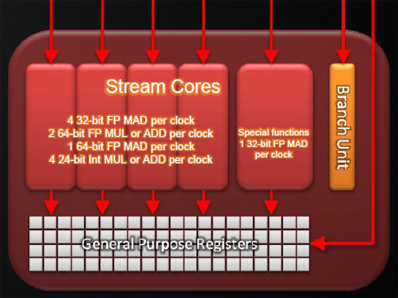
Inside each of the VLIW superscalar thread processors, there are five execution units, a branch prediction unit and a set of general purpose registers. Of the five units in each in each superscalar thread processor, there are four units which can handle a limited number of instructions per clock cycle and a fifth 'special function' unit. The four 'standard' FPUs can handle the following instructions per clock cycle:

A Cypress (RV870) thread processor
- Four 32-bit FP MAD
- Two 64-bit FP MUL or ADD
- One 64-bit MAD; or
- Four 24-bit Int MUL or ADD
Each FPU can handle DOT products and SAD (sum of absolute differences) instructions as well. AMD said that DOT products are much more flexible in Cypress, while the SAD instruction enables some significant speed ups. It's mainly used for general purpose compute operations, especially video encoding, where AMD says it has seen a 12x speed up using the native instruction.
This hasn’t been exposed in either OpenCL or DirectX, but AMD has exposed it to developers via a backdoor. It can be used via library functions such as those available in the AMD media library (which is available to developers developing video encoding applications) and will also be an OpenCL extension. AMD said that it has tweaked its compiler so that it’s able to recognise a sequence of instructions and replace them with a SAD instruction. This is currently in beta testing, so isn't exposed yet, but AMD said that it will be available very soon.

The cores haven't changed a great deal from RV770
IPC has also been improved in general terms, too, and that's largely thanks to the introduction of co-issuing a MUL instruction with a dependent ADD instruction in a single clock cycle. Fused multiply-add has also been added to further improve IPC, as it enables a multiply-add (MAD) operation to be performed in a single cycle, with a single rounding.
The branch execution unit is also present inside Cypress and it is again tasked with the same flow control and conditional operations, but AMD chooses not to count this when tallying up the number of FPUs. Register space also remains unchanged at the thread processor level, but obviously because the number of cores (and so, thread processors) has doubled, total register space has increased by the same factor.

MSI MPG Velox 100R Chassis Review
October 14 2021 | 15:04


Want to comment? Please log in.