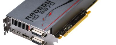
Radeon HD 6870 Specifications
The Barts design, also known as the Radeon HD 6800
In fact, the Barts design of the HD 6800 series (right) is fairly conservative – an effort, no doubt, to deliver the chip on time and to a particular budget. After all, even Intel doesn’t take on the project of designing a whole new architecture as well as proving a new manufacturing process, and yet the GPU world has been doing this for years.
This is possibly a sign of GPU design and production maturing and trying to avoid lengthy delays on new products, or perhaps it’s just that we’re getting to the point where manufacturing shrinks are so complicated that we won’t see the rapid shrinking of the mid-Naughties. Or possibly it’s a bit of both.
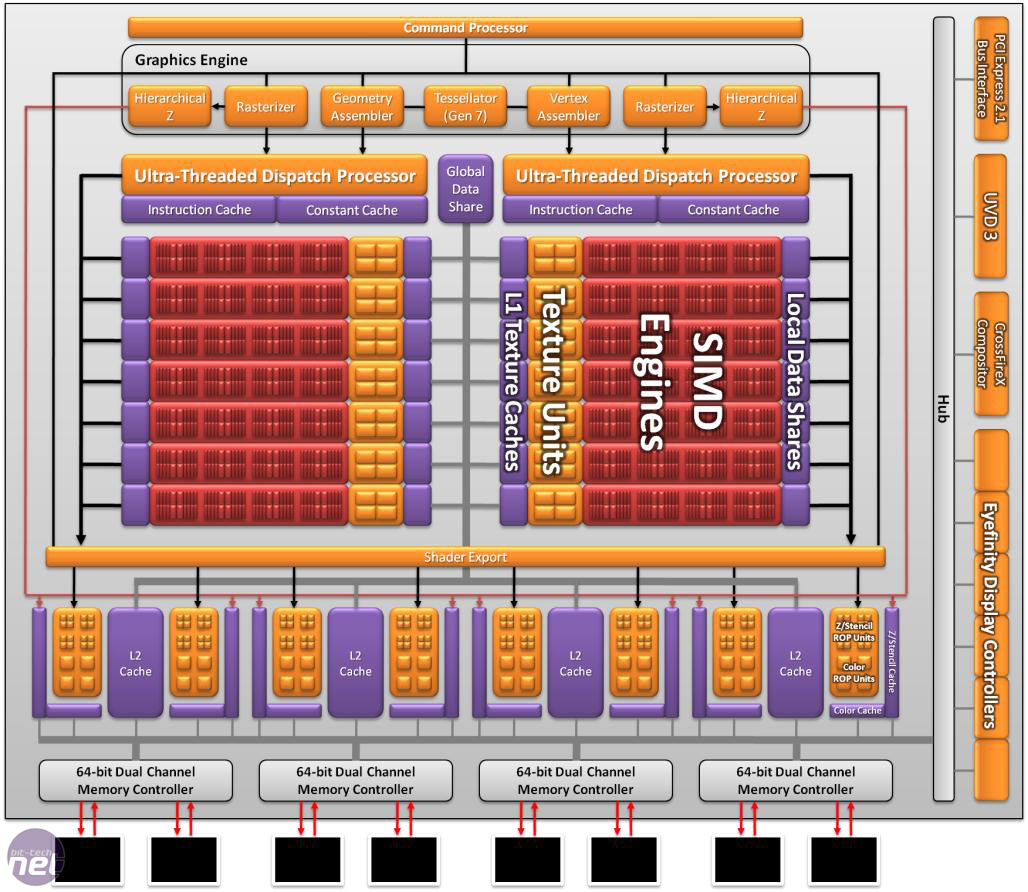
Either way, the bulk of a HD 6870 1GB looks very familiar to anyone who knows their ATI hardware – there’s a huge bank of SIMD (Single Instruction, Multiple Data) engines with 80 stream processors each. These stream processors follow the VLIW5 (Very Long Instruction Word, 5:1 ratio) configuration of having a super stream processor for every five basic units, with this unit capable of double-precision floating point operations and other high-precision maths.
The total number of stream processors in the Barts GPU is 1,120, the same as a Radeon HD 5830 1GB, but the Barts design has an upgraded front end to keep those stream processors working. This upgrade is combined with much higher GPU frequencies to deliver more performance – this is despite HD 6800 GPUs using the same 40nm manufacturing process as the HD 5000-series. The HD 6870 1GB has a clock speed of 900MHz and is complemented by 1GB of 1,050MHz (4.2GHz effective) DDR5 memory while the HD 6850 1GB has a frequency of 775MHz and 1GB of 1GHz (4GHz effective) GDDR5 memory.In comparison a HD 5850 1GB has a clock speed of 725MHz and 1GHz (4GHz effective) GDDR5 memory.
A New Front End?
With tessellation one of the stand-out features of DirectX 11, we were expecting ATI to add more grunt in this department, and our expectations were duly met. However, we expected a little more than the incremental updates of Barts’ tessellation engine, which only offers better thread management and buffering over and beyond the tessellation unit of the HD 5000-series. This means that while Nvidia’s Fermi GPUs have tessellation units galore (one per SM, with three or four SMs per GPC and one to four GPCs per chip), a HD 6800 GPU still only has one. ATI still claims that the HD 6870 has up to twice the tessellation performance of a HD 5870, however.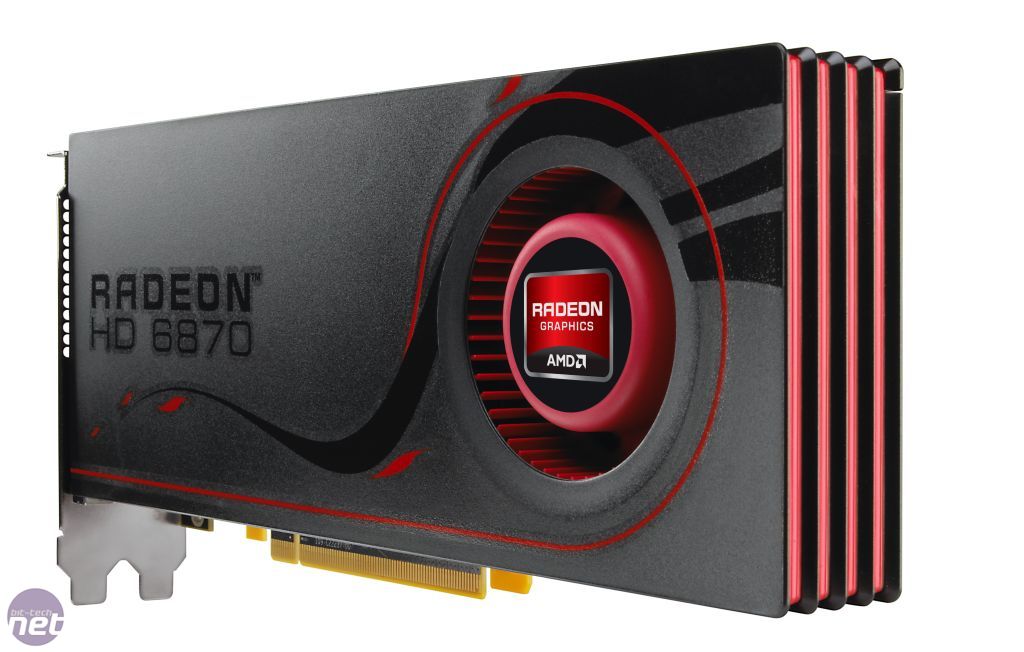
Click to enlarge
ATI also claims that the geometry throughput of the HD 6800 series has been improved, but this is merely because of the higher GPU frequency of a HD 6870. A HD 5850 manages to process 725 million polygons per second thanks to its 725MHz frequency while a HD 6870 can process 900 million polygons per second as it’s clocked at 900MHz. While the front end of a HD 6800 GPU has a new design, it’s a fairly small and incremental update from the Evergreen GPU design of the HD 5000-series.
The back end of Barts is identical to that of the HD 5800 GPU on paper, with a 256-bit memory interface and 32 ROPs. While we’re used to seeing effective memory frequencies of 4.8GHz from even lower mid-range cards such as the HD 5770 1GB, the HD 6870 1GB only has an effective memory frequency of 4.2GHz while the HD 6850 1GB has the same 4GHz effective frequency as the HS 5850 1GB,
| ATI Radeon HD 5870 1GB | ATI Radeon HD 6870 1GB | ATI Radeon HD 5850 1GB | ATI Radeon HD 6850 1GB | ATI Radeon HD 5770 1GB | Nvidia GeForce GTX 470 1,280MB | Nvidia GeForce GTX 460 1GB | Nvidia GeForce GTX 460 768MB | |
| GPU | ||||||||
| Codename | Cypress XT | Barts XT | Cypress Pro | Barts Pro | Juniper XT | GF100 | GF104 | GF104 |
| Frequency | 850MHz | 900MHz | 725MHz | 775MHz | 850MHz | 607MHz | 675MHz | 675MHz |
| Stream Processors | 1,600 (850MHz) | 1,120 (900MHz) | 1,440 (725MHz) | 980 (775MHz) | 800 (850MHz) | 448 (1,215MHz) | 336 (1,350MHz) | 336 (1,350MHz) |
| Layout | 20 SIMD engines | 14 SIMD engines | 18 SIMD engines | 12 SIMD engines | 10 SIMD engines | 14 SMs, 4 GPCs | 7 SMs, 2 GPCs | 7 SMs, 2 GPCs |
| Rasterisers | 2 | 2 | 2 | 2 | 2 | 4 | 2 | 2 |
| Tesselation Units | 1 | 1 | 1 | 1 | 1 | 14 | 7 | 7 |
| Texture Units | 80 | 56 | 72 | 48 | 40 | 56 | 7 | 7 |
| ROPs | 32 | 32 | 32 | 32 | 16 | 40 | 32 | 24 |
| Transistors | 2.15bn | 1.7bn | 2.15bn | 1.7bn | 1.04bn | 3bn | 1.95bn | 1.95bn |
| Size | 334mm2 | 255mm2 | 334mm2 | 255mm2 | 166mm2 | 530mm2 | 348mm2 | 348mm2 |
| Process | 40nm | 40nm | 40nm | 40nm | 40nm | 40nm | 40nm | 40nm |
| Memory | ||||||||
| Amount | 1GB GDDR5 | 1GB GDDR5 | 1GB GDDR5 | 1GB GDDR5 | 1GB DDR5 | 1,280MB GDDR5 | 1GB GDDR5 | 768MB GDDR5 |
| Frequency | 1,050MHz (4.2GHz effective) | 1,050MHz (4.2GHz effective) | 1GHz (4GHz effective) | 1GHz (4GHz effective) | 1.2GHz (4.8GHz effective) | 837MHz (3.2GHz effective) | 900MHz (3.6GHz effective) | 900MHz (3.6GHz effective) |
| Interface | 256-bit | 256-bit | 256-bit | 256-bit | 128-bit | 320-bit | 256-bit | 192-bit |
| Bandwidth | 134.4 GB/sec | 134.4 GB/sec | 128 GB/sec | 128 GB/sec | 76.8 GB/sec | 134 GB/sec | 115 GB/sec | 86 GB/sec |
| Card Specifications | ||||||||
| Power Connectors | 2 x 6-pin PCI-E | 2 x 6-pin PCI-E | 2 x 6-pin PCI-E | 1 x 6-pin PCI-E | 1 x 6-pin PCI-E | 2 x 6-pin PCI-E | 1 x 6-pin PCI-E | 1 x 6-pin PCI-E |
| Max Power Draw | 188W | 151W | 151W | 127W | 108W | 215W | 160W | 150W |
| Idle Power Draw | 27W | 19W | 27W | 19W | Unknown | Unknown | Unknown | Unknown |
| Rec PSU | 500W | Unknown | 500W | Unknown | 450W | 550W | 450W | 450W |
| Rough Street Price | £320 | £220 | £200 | £150 | £120 | £200 | £155 | £120 |


MSI MPG Velox 100R Chassis Review
October 14 2021 | 15:04

Want to comment? Please log in.