Speeds and feeds
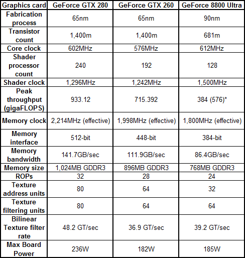
As with G80 and its derivatives, there are three clock speeds that Nvidia talks about inside its architecture. The company has said on multiple occasions that there are many more clock domains inside its GPUs, but it prefers not to talk about them.The shader processors in the GeForce GTX 280 run at 1,296MHz, while the core clock sits at 602MHz – this clock is responsible for the instruction dispatch, set up engine, texture units and ROPs.
The final clock that Nvidia discusses is the memory speed, which is set to 1,107MHz (2,214MHz effective) on the flagship part. Combined with the 512-bit memory interface, this results in an impressive memory bandwidth of approximately 141.7GB per second.

* There are very few instances where G80 can hit the higher peak throughput rate
Thus far we haven’t talked much about the GeForce GTX 260 – that’s mainly because we’ll be talking more about that particular card in a later article. However, for the sake of completeness, its shader core runs at 1,242MHz, core is set to 576MHz and the memory clock is 999MHz (1,998MHz).
It’s also worth bearing in mind that the GeForce GTX 260 also features a cut-down design, where two of the ten texture processing clusters and one of the ROP partitions are disabled, meaning that the GeForce GTX 260 features only 192 shader processors, 64 texture units and 28 ROPs backing out onto a 448-bit memory interface and 896MB of GDDR3 memory.

Despite the narrower memory interface, the GeForce GTX 260 still delivers some impressive statistics. At peak, the cut down GTX 260 delivers over 715 gigaFLOPS of compute power, 36.9 gigatexels per second of texture fill rate and almost 112GB per second of memory bandwidth – they’re impressive numbers in their own right.
Let's dive a little deeper and have a look at some theoretical throughputs...

MSI MPG Velox 100R Chassis Review
October 14 2021 | 15:04


Want to comment? Please log in.