Nvidia GeForce GTX 460 768MB Review
Manufacturer: NvidiaUK price (as reviewed): £179 (inc VAT) MSRP
US price (as reviewed): $199 (ex tax) MSRP
Not content with launching the GeForce GTX 465 roughly six weeks ago, Nvidia has launched two more today. Or rather it’s launched one more, though there are two versions of it – the GeForce GTX 460 1GB and the lesser GTX 460 768MB. The aim is clear – Nvidia has had a bad run of late, and it needs to halt the succession of poor reviews with something that’ll make people sit up and care about the name GeForce again.
The GTX 460 looks like the card to do it, if only on paper, as the specs are more than we’d expected. Typically the mid-range GPU of a family has about half the resources of the top-end GPU, but the GTX 460 has roughly 70 per cent of the stream processors of the GTX 480 at 336 versus 480. To understand why we were surprised, and why there are two models of the GTX 460, we need to recap on the unusual way that Nvidia has designed it DX11 GPUs. Alternatively, if you already know your Raster Engine from your Polymorph, skip to page two for the architectural updates in the new GF104 GPU.
Fermi 101
All modern GPUs are structured around a basic layout – there’s a front-end that accepts work from the CPU and splits into a load of separate work threads. These threads then get fed into a bank of stream processors, and after being processed by these, are sent to the frame buffer via the ROPs and memory controller.In a Fermi GPU, the stream processors are organised in clusters (called SMs, or Streaming Multiprocessors, in Nvidian) and these SMs are organised into groups of three or four to make the basis of what Nvidia calls GPCs. GPCs are more than just groups of SMs though, they’re pretty much mini-GPUs. Each GPC has a Raster Engine, which does the basic setup elements to the data given to it by the GigaThread dispatch engine, ready for the stream processors to work on. Each stream processor cluster has its own PolyMorph Engine, which contains a tesselator unit, again an element that you’d expect to find in the front end of GPU. The GPCs output to, and communicate via, a Level 2 cache that runs through the centre of the chip.
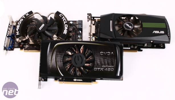
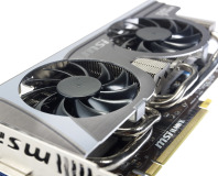
Manufacturers were keen to send us their GTX 460 cards, which is usually a sign that a product is rather good. Click to enlarge.
The benefits of this design are two-fold: there’s a degree of modularity, as you can just cut GPCs from the full-fat GF100 design to produce lesser versions to hit lower price-points more keenly, and there’s a distributed design that Nvidia claims is ideal for tessellation. The reason for this claim is that, as tessellation is a vertex operation (tesselation adds extra geometry detail on-the-fly for less angular objects and characters) the results of a tessellation operation need to be fed back through a setup stage for the stream processors to be able to work on them. If the tesselator units were in a large monolithic front-end, tessellation could lead to the front-end refusing new work and the GPU stalling.

MSI MPG Velox 100R Chassis Review
October 14 2021 | 15:04



Want to comment? Please log in.