Nvidia GeForce GTX 460 1GB Review
Manufacturer: NvidiaUK price (as reviewed): £199 (inc VAT) MSRP
US price (as reviewed): $229 (ex tax) MSRP
It’s not been fun being green for the last ten months or so – ATI has been dominant in the DX11 fight, with Nvidia late with its first next-gen GPUs. Worse still, when these did arrive, they were hot, noisy, power-hungry and not as fast as anyone had hoped. The underwhelming launch of the GeForce GTX 470 and the GeForce GTX 480 was followed by the woeful GeForce GTX 465.
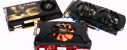
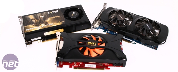
Clearly Nvidia is keen to change this sequence of events, and the GeForce GTX 460 looks like the card to do just that. While the GTX 465 was in reality a hugely cut-down GTX 480 (based on the full GF100 Fermi design) the GTX 460 is built from scratch to be a mid-range, high-performance GPU. The new GPU is codenamed GF104, and is the first example of one of the design aims of the Fermi architecture – modularity. As the Fermi architecture is a rather odd one, let’s have a refresh of how it’s laid out.
Then again, if you’re pretty comfortable with the uniqueness of Nvidia’s Fermi architecture, you could skip to page two to read about the two versions of the GTX 460 and what the differences are.
Fermi 101
All modern GPUs are structured around a basic layout – there’s a front-end that accepts work from the CPU and splits into a load of separate work threads. These threads then get fed into a bank of stream processors, and after being processed by these, are sent to the frame buffer via the ROPs and memory controller.In a Fermi GPU, the stream processors are organised in clusters (called SMs, or Streaming Multiprocessors, in Nvidian) and these SMs are organised into groups of three or four to make the basis of what Nvidia calls GPCs. GPCs are more than just groups of SMs though, they’re pretty much mini-GPUs.
Each GPC has a Raster Engine, which does the basic setup elements to the data given to it by the GigaThread dispatch engine, ready for the stream processors to work on. Each stream processor cluster has its own PolyMorph Engine, which contains a tesselator unit, again an element that you’d expect to find in the front end of GPU. The GPCs output to, and communicate via, a Level 2 cache that runs through the centre of the chip.
The benefits of this design are two-fold: there’s a degree of modularity, as you can just cut GPCs from the full-fat GF100 design to produce lesser versions to hit lower price-points more keenly, and there’s a distributed design that Nvidia claims is ideal for tessellation.
The reason for this claim is that, as tessellation is a vertex operation (tesselation adds extra geometry detail on-the-fly for less angular objects and characters) the results of a tessellation operation need to be fed back through a setup stage for the stream processors to be able to work on them. If the tesselator units were in a large monolithic front-end, tessellation could lead to the front-end refusing new work and the GPU stalling.

MSI MPG Velox 100R Chassis Review
October 14 2021 | 15:04


Want to comment? Please log in.