The GM206 GPU
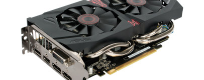
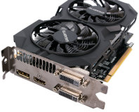
As with the GTX 970 launch, Nvidia has not produced a reference board, and went straight to a virtual design. As such, for water-cooling enthusiasts out there, you'll need to do some careful research to find compatible waterblocks. This is also a hard launch, with multiple SKUs from numerous board partners available immediately. We're featuring Asus for this launch article, with more to follow in the coming days and weeks.| Nvidia GeForce GTX 980 4GB | Nvidia GeForce GTX 970 4GB | Nvidia GeForce GTX 960 2GB | Nvidia GeForce GTX 660 2GB | Nvidia GeForce GTX 750 Ti 2GB | |
| GPU | |||||
| Architecture | Maxwell | Maxwell | Maxwell | Kepler | Maxwell |
| Codename | GM204 | GM204 | GM206 | GK106 | GM107 |
| Base Clock | 1,126MHz | 1,050MHz | 1,127MHz | 980MHz | 1,020MHz |
| Boost Clock | 1,216MHz | 1,178MHz | 1,178MHz | 1,033MHz | 1,085MHz |
| Stream Processors | 2,048 | 1,664 | 1,024 | 960 | 640 |
| Layout | 4 GPCs, 16 SMMs | 4 GPCs, 13 SMMs | 2 GPCs, 8 SMMs | 3 GPCs, 5 SMXs | 1 GPC, 5 SMMs |
| Rasterisers | 4 | 4 | 2 | 3 | 1 |
| Tesselation Units | 16 | 13 | 8 | 5 | 5 |
| Texture Units | 128 | 104 | 64 | 80 | 40 |
| ROPs | 64 | 64 | 32 | 24 | 16 |
| Transistors | 5.2 billion | 5.2 billion | 2.94 billion | 2.54 billion | 1.87 billion |
| Die Size | 398mm2 | 398mm2 | 227mm2 | 221mm2 | 148mm2 |
| Process | 28nm | 28nm | 28nm | 28nm | 28nm |
| Memory | |||||
| Amount | 4GB GDDR5 | 4GB GDDR5 | 2GB GDDR5 | 2GB GDDR5 | 2GB GDDR5 |
| Frequency | 1.75GHz (7GHz Effective) | 1.75GHz (7GHz Effective) | 1.75GHz (7GHz Effective) | 1.5GHz (6GHz effective) | 1.35GHz (5.4GHz effective) |
| Interface | 256-bit | 256-bit | 128-bit | 192-bit | 128-bit |
| Bandwidth | 224GB/sec | 224GB/sec | 112GB/sec | 144GB/sec | 86.4GB/sec |
| Card Specifications | |||||
| Power Connectors | 2 x 6-pin PCI-E | 2 x 6-pin PCI-E | 1 x 6-pin PCI-E | 1 x 6-pin PCI-E | None |
| Stock Card Length | 267mm | 267mm | N/A | 241mm | 147mm |
| TDP | 165W | 145W | 120W | 140W | 60W |
The reference display outputs from the GTX 980 are carried over, namely three DisplayPort 1.2 connections, a dual-link DVI-I and HDMI 2.0, which is a newcomer for this market segment. The GTX 960 also features Nvidia's new display engine, with support for up to 5K resolutions and a maximum of four monitors, including four 4K MST displays. A new addition is H.265 encode and decode (previously encode only on the GTX 980), which may appeal to home threatre users, as well as native support for HDCP 2.2 content protection over HDMI.
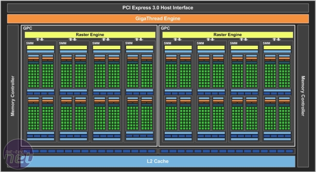
On to the nitty gritty details, the GTX 960 utilises a new GPU called GM206, the direct successor to the Kepler-based GK106 used by the GTX 660. It is of course a 28nm part with 2.94 billion transistors and a 227mm2 die size. It uses the same Maxwell streaming multiprocessor (SMM) design introduced with the GTX 980 (see here for the full details), whereby each SMM has four blocks of 32 CUDA cores. GM206 has two graphics processing clusters (GPCs) with four SMMs apiece, for a total of 1,024 CUDA cores and 64 texture units. This is only 7 percent more cores than the GTX 660, and 128 less than GTX 760 (and less texture units than both too). However, the efficiency of the SMM design means the cores are utilised a lot more, with Nvidia saying that each GM206 core does approximately 1.4 times the work of a GK106 core, and delivers roughly twice the performance-per-watt. The reference base clock speed is 1,127MHz, with a rated boost clock of 1,178MHz – expect this to vary significantly depending on board partner and SKU.
As you can see, there are only two memory controllers in the GM206 GPU, giving it a 128-bit interface compared to 192-bit on GTX 660 and 256-bit on GTX 760. The use of faster memory is one simple way to help overcome this, with 7GHz being the default speed. L2 cache has also been massively increased, from 384KB to 1MB, reducing the number of calls to the GDDR5 memory. Speaking of, the GTX 960 has a 2GB frame buffer. No 4GB variants have yet been confirmed.
Finally, GTX 960 also utilises Nvidia's third-generation delta colour compression, a lossless compression algorithm that leads to, on average, 25 percent fewer bytes per frame and thus a memory interface that is a third faster than Kepler's (again, on average). This has led to Nvidia quoting its raw 112GB/sec memory bandwidth as 148.8GB/sec “effective”, which is a little higher than the GTX 660's 144.2GB/sec and thus not a downgrade – either way, the results should show us whether the lower interface is a limiting factor. Finally, with 16 ROPs per memory controller now, these have increased from 24 to 32 total.

MSI MPG Velox 100R Chassis Review
October 14 2021 | 15:04



Want to comment? Please log in.