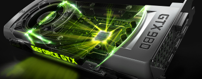
GM204: Maxwell Fully Realised
The GM107 chip inside the GTX 750 Ti was referred to at the time as a first generation Maxwell part. GM204, meanwhile, is the start of the second generation and is essentially the full realisation of the architecture. 5.2 billion transistors have been crammed into the 398mm2 die. As mentioned, it's manufactured using the same (albeit now very mature) TSMC 28nm process as that which Kepler was first built on. Delays in the development of the 20nm process are responsible, but even on this same process Nvidia has been able to make significant efficiency gains.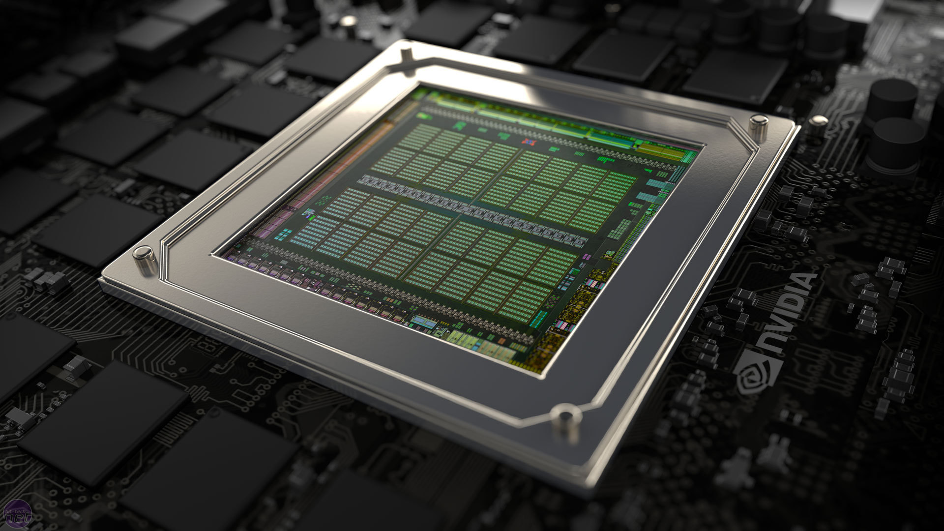
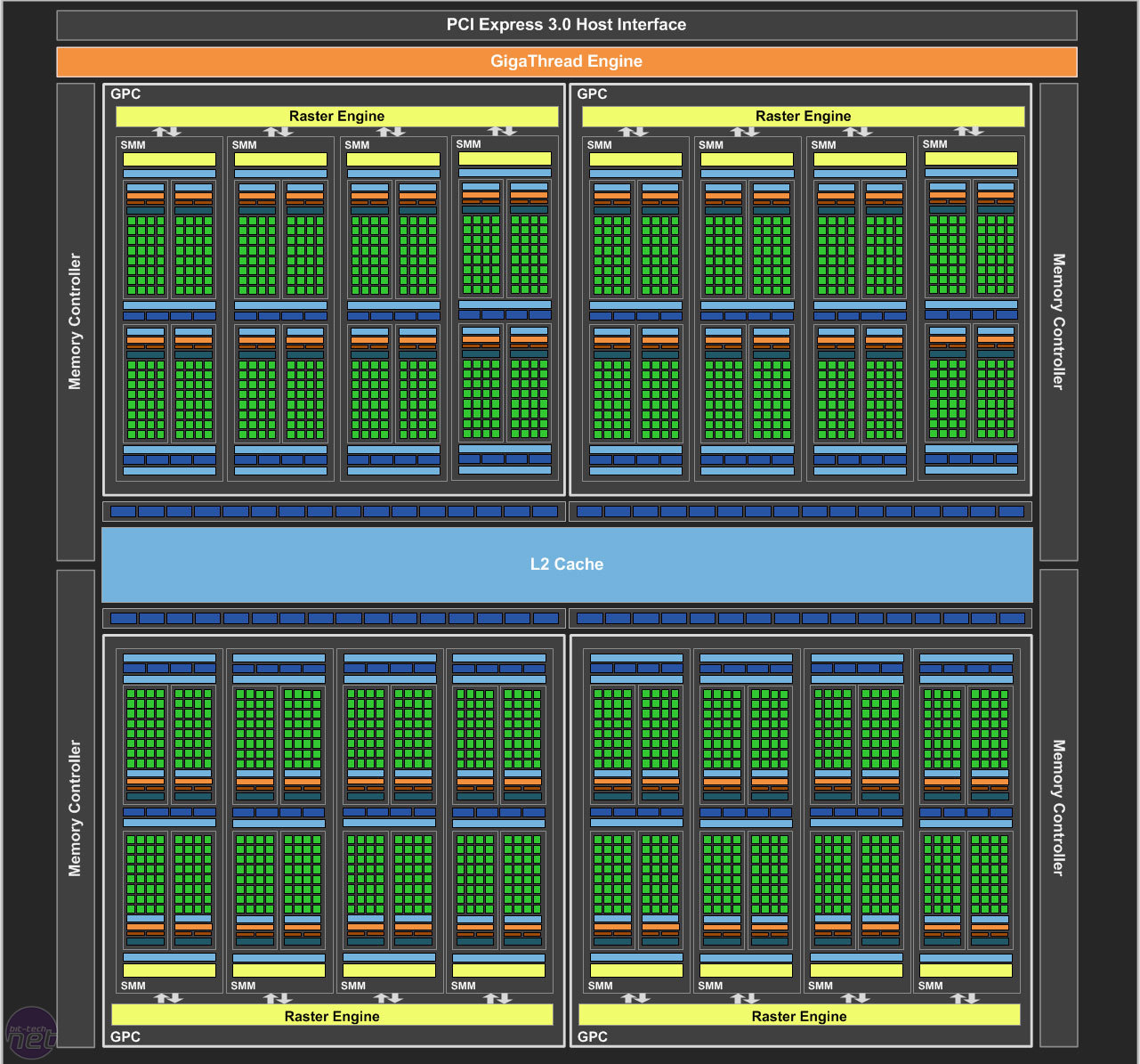
Click to enlarge - The GM204 die and block diagram
The main building blocks of GM204 are Nvidia's redesigned streaming multiprocessors, now referred to as SMMs, which are arranged into Graphics Processing Clusters, or GPCs. The SMMs have the same design as those in GM107, and you can read more about them in our coverage of the GTX 750 Ti. Essentially, however, Nvidia cut the CUDA core count from 192 in Kepler to 128, and split these into four blocks of 32, each with its own warp and scheduling hardware. Reorganising the data path into a simpler, power-of-two structure like this allowed the cores to be fully utilised more often and improved scheduling efficiency by reducing the need for the complex resource sharing required in Kepler, where the warp and scheduling hardware had access to all 192 cores. Ultimately, Nvidia improved performance per core by around 35-40 percent in shader limited workloads, effectively double performance per watt over Kepler and maintained around 90 percent of performance with just two thirds of the original core count.

Click to enlarge - a Maxwell SMM
Clock speeds have also been given a bump. In fact, the GTX 980 ships with Nvidia's highest clock speeds yet. The GPU has a base clock of 1,126MHz, and a rated boost clock of 1,216MHz. This boost clock can be considered an average of sorts; the actual boost frequency you see depends on a number of factors including power, temperature and workload requirements. In our own testing, we found it would boost to a maximum of 1,240MHz, but stayed on average between 1,177MHz and 1,200MHz.
Those of you with an eye for detail may have noticed that GM204 has the same number of texture units as GK104 – there are twice as many SMs in the new GPU, but Maxwell SMs have half as many texture units (eight) as their Kepler counterparts. The reason for this is, as you might have expected, efficiency. Nvidia found that eight texture units offered the most efficient balance of math and texture processing for today's games. Also, the 12 percent higher clock speed of GM204 means that texture fill rate is up by the same amount.
Four 64-bit memory controllers grant the GTX 980 a 256-bit memory interface, the same as the GTX 680 and actually less than the GK110 parts (GTX 780, GTX 780 Ti and the GTX Titan family). However, Nvidia has a few ways of preventing this relatively narrow interface from becoming a bottleneck. First is simply the use of fast memory; all GTX 980 parts will ship with its GDDR5 clocked at 1.75GHz (7GHz effective), the joint highest within Nvidia's line-up. As such, memory bandwidth stands at 224GB/sec, a respectable but not outstanding figure.
Next is the size of the onboard L2 cache, which is a whopping 2MB (512KB aligned with each memory controller). This is the same as that of the GTX 750 Ti, but it's also bigger than any other card on the market, including the GTX Titan range. The result of so large a cache is less reliance on the comparatively slow and power-hungry off-chip memory and less demand on the memory bus.
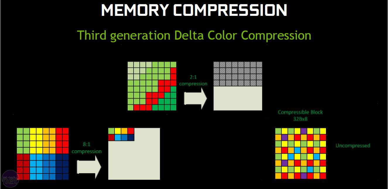
Click to enlarge
Finally, for when GM204 does need to access the off-chip GDDR5, Nvidia has introduced third generation delta colour compression, similar to what we saw in AMD's Tonga GPU with the R9 285. It is essentially a lossless method of compressing frame data to reduce the memory bandwidth requirements when writing to (and later when reading from) memory, and this third generation of the process gives the compressor more choices when calculating delta values. Nvidia found that in most cases, the majority of frame data can be compressed, and there is no performance penalty for doing so. There is also no image quality reduction since it must always be lossless – if this isn't possible, it will be written uncompressed. According to Nvidia, the result of the technique is a reduction of bytes needed from memory per frame of around 25 percent on average.
Like L2 cache segments, ROPs are again aligned with the memory controllers. In GM107, we saw eight ROPs for each of the two controllers, but in GM204 there are 16 per controller for a total of 64 ROPs. This is double the count of the GTX 680, and with the higher clock speeds pixel fill rate is more than doubled. This, along with the doubling of the frame buffer from 2GB to 4GB, equips the GTX 980 for 4K gaming.
RELATED ARTICLES


MSI MPG Velox 100R Chassis Review
October 14 2021 | 15:04

Want to comment? Please log in.