
At the start of last month, we had a look at NVIDIA’s brand new GeForce 8800 GTX and also looked closely at the architecture behind NVIDIA’s G80 graphics processor. On virtually all accounts, the GeForce 8800 GTX is a simply phenomenal video card that is capable of delivering a fantastic gaming experience in today’s most intensive games at resolutions all the way up to 2560x1600.
That kind of performance comes at a massive cost though, with retail GeForce 8800 GTX cards approaching £450 in the UK once you add the tax man’s share on top. Today, we are having a look at NVIDIA’s GeForce 8800 GTS – a slightly more affordable GeForce 8800 series video card with retail prices spreading between £300-350 including VAT. The GTS moniker has not been used since GeForce 2 GTS when it meant Giga-Texel Shading. This time around it doesn’t have a meaning, but it’s good to see NVIDIA bring back an old favourite of mine.
Before we go much further, we’re going to take a lot of what we covered in our GeForce 8800 GTX review and architectural overview as somewhat common knowledge, so it’s recommended that you familiarise yourself with the architecture if you haven’t already.
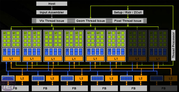
The GeForce 8800 GTS pipelineNVIDIA has cut the number of stream processors from 128 to 96 – a 25% reduction; this reduction in stream processors also affects the number of texture address and filtering units. The result is that the texture address unit capacity is down from 32 to 24, while the texture filtering capacity is reduced from 64 to 48.
In addition, NVIDIA cut one of the ROP partitions out on 8800 GTS, leaving 20 of the original 24 ROPs enabled. Inside the G80 graphics processor, each ROP partition (each containing four ROPs) has access to a 64-bit memory interface and two DRAM chips. As a result of reducing the number of ROP partitions from six to five, the memory bus width has been reduced from 384-bit down to 320-bit.
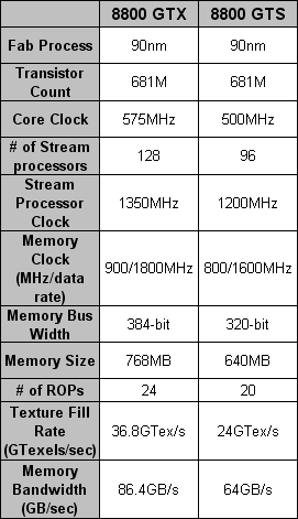 On top of cutting down on some of the parallelism inside the GeForce 8800 GTS GPU, NVIDIA has also reduced the clock speeds on the 8800 GTS, too. The core clock, which covers the setup/dispatch unit, along with the texture units and ROP partitions of the G80 pipeline, has been reduced from 575MHz to 500MHz. NVIDIA also decided to reduce the stream processor clock from 1350MHz down to 1200MHz, while the memory clock was also down graded from 900/1800MHz to 800/1600MHz.
Although the lower clock speeds may not seem to matter all that much, each contributes to a considerably slower GPU on paper. The result of having 25% fewer stream processors at a lower shader clock means that GeForce 8800 GTS only has two thirds the raw shader power of the 8800 GTX. Secondly, the lower core clock combined with fewer texture units means the GTS has just over 65% of the texture fillrate throughput. Finally, the 100MHz lower memory clock equates to a 22.4GB/sec memory bandwidth deficit when you combine it with the narrower memory bus width on the GeForce 8800 GTS.
G80 has around 681M transistors packed into a ~420mm² die, making it over two times the size of G71, which had 278M transistors and a 196mm² surface area. Taking the size and complexity of G80 into account, it’s fair to say that yield may not be as high as NVIDIA would like, and there are going to be quite a few defective cores on each wafer. In that respect, it makes sense for NVIDIA to use as many of these cores as possible, explaining why NVIDIA opted for the ‘cut down’ route this time around.
The same was true with G70, which had a large 334mm² die (considered large at that time) manufactured on TSMC’s 110nm process and NVIDIA chose to make GeForce 7800 GT a cut-down version of GeForce 7800 GTX, with only 20 pixel pipelines and seven vertex shaders enabled. However, things changed when NVIDIA shrunk G70 to 90nm, creating G71 and the GeForce 7900 series. Because the die size was massively reduced, NVIDIA was able to ship GeForce 7900 GT with all portions of the GPU enabled, but at much lower clock speeds than the flagship GeForce 7900 GTX.
When NVIDIA gets around to shrinking G80 to a smaller process node, it’s possible that – if recent history repeats itself – the company will ship its second fastest part (at the time) with all portions of the GPU enabled, but with much lower clock speeds (and possibly less memory) than the flagship product.
That kind of performance comes at a massive cost though, with retail GeForce 8800 GTX cards approaching £450 in the UK once you add the tax man’s share on top. Today, we are having a look at NVIDIA’s GeForce 8800 GTS – a slightly more affordable GeForce 8800 series video card with retail prices spreading between £300-350 including VAT. The GTS moniker has not been used since GeForce 2 GTS when it meant Giga-Texel Shading. This time around it doesn’t have a meaning, but it’s good to see NVIDIA bring back an old favourite of mine.
Before we go much further, we’re going to take a lot of what we covered in our GeForce 8800 GTX review and architectural overview as somewhat common knowledge, so it’s recommended that you familiarise yourself with the architecture if you haven’t already.
GeForce 8800 GTS in a nutshell...
Although GeForce 8800 GTS is based on the same G80 graphics processing unit, it’s quite a different beast from its big brother, GeForce 8800 GTX which is NVIDIA’s all-bells-all-whistles 8800-series video card. There are immediately obvious cosmetic differences that are as a result of the not-so-obvious architectural differences that have collectively helped to reduce the card’s retail price.The GeForce 8800 GTS pipeline
In addition, NVIDIA cut one of the ROP partitions out on 8800 GTS, leaving 20 of the original 24 ROPs enabled. Inside the G80 graphics processor, each ROP partition (each containing four ROPs) has access to a 64-bit memory interface and two DRAM chips. As a result of reducing the number of ROP partitions from six to five, the memory bus width has been reduced from 384-bit down to 320-bit.
On top of cutting down on some of the parallelism inside the GeForce 8800 GTS GPU, NVIDIA has also reduced the clock speeds on the 8800 GTS, too. The core clock, which covers the setup/dispatch unit, along with the texture units and ROP partitions of the G80 pipeline, has been reduced from 575MHz to 500MHz. NVIDIA also decided to reduce the stream processor clock from 1350MHz down to 1200MHz, while the memory clock was also down graded from 900/1800MHz to 800/1600MHz. Although the lower clock speeds may not seem to matter all that much, each contributes to a considerably slower GPU on paper. The result of having 25% fewer stream processors at a lower shader clock means that GeForce 8800 GTS only has two thirds the raw shader power of the 8800 GTX. Secondly, the lower core clock combined with fewer texture units means the GTS has just over 65% of the texture fillrate throughput. Finally, the 100MHz lower memory clock equates to a 22.4GB/sec memory bandwidth deficit when you combine it with the narrower memory bus width on the GeForce 8800 GTS.
G80 has around 681M transistors packed into a ~420mm² die, making it over two times the size of G71, which had 278M transistors and a 196mm² surface area. Taking the size and complexity of G80 into account, it’s fair to say that yield may not be as high as NVIDIA would like, and there are going to be quite a few defective cores on each wafer. In that respect, it makes sense for NVIDIA to use as many of these cores as possible, explaining why NVIDIA opted for the ‘cut down’ route this time around.
The same was true with G70, which had a large 334mm² die (considered large at that time) manufactured on TSMC’s 110nm process and NVIDIA chose to make GeForce 7800 GT a cut-down version of GeForce 7800 GTX, with only 20 pixel pipelines and seven vertex shaders enabled. However, things changed when NVIDIA shrunk G70 to 90nm, creating G71 and the GeForce 7900 series. Because the die size was massively reduced, NVIDIA was able to ship GeForce 7900 GT with all portions of the GPU enabled, but at much lower clock speeds than the flagship GeForce 7900 GTX.
When NVIDIA gets around to shrinking G80 to a smaller process node, it’s possible that – if recent history repeats itself – the company will ship its second fastest part (at the time) with all portions of the GPU enabled, but with much lower clock speeds (and possibly less memory) than the flagship product.
RELATED ARTICLES


MSI MPG Velox 100R Chassis Review
October 14 2021 | 15:04

Want to comment? Please log in.