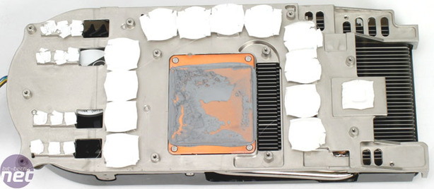
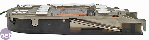
G80: NVIDIA GeForce 8800 GTX

Written by Tim Smalley

November 8, 2006 | 18:59

Tags: #8800 #benchmark #evaluation #experience #g80 #gameplay #geforce #gtx #performance #pictures #review #score

Companies: #nvidia

Under the heatsink

G80: NVIDIA GeForce 8800 GTX Under the heatsink
Unscrewing the hefty cooler from the board shows a busy thermal interface underneath. There are a large number of white pads, designed to sit on top of the memory chips - there is 768MB of memory on this reference card, and that requires a massive twelve memory chips built on to the front of the card in three blocks of four. At the rear of the cooler there is a thermal interface to some of the power regulation circuitry to help keep the card stable, as well as some more traditional thermal paste covering the main GPU core.

The twelve memory chips on the GeForce 8800 GTX split down into six 64-bit memory channels (with two DRAMs per channel), combining for a total 384-bit memory interface width. The memory crossbar design is very similar to the design used in GeForce 7-series hardware, and comes complete with support for DDR1, DDR2, DDR3, GDDR3 and GDDR4 memory types. Currently, NVIDIA is using GDDR3 memory on both GeForce 8800 GTX and 8800 GTS – how long do you think it’ll be before NVIDIA launches a GDDR4 version?

G80: NVIDIA GeForce 8800 GTX Under the heatsink
G80: NVIDIA GeForce 8800 GTX Under the heatsink G80: NVIDIA GeForce 8800 GTX Under the heatsink
You can see that the GPU core dominates the surface of the board - it's massive, far larger than any GPU we've seen previously. The heatspreader on top lacks any particular identifying markings - there's a disappointing lack of 'G80' anywhere on there for bragging rights. It's made on TSMC's 90nm manufacturing process and has a massive 681 million transistors under the hood - we told you it was the most complex graphics chip ever made - it's more than double the number of transistors in a single G71.

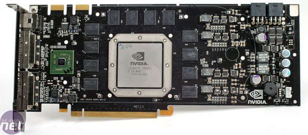
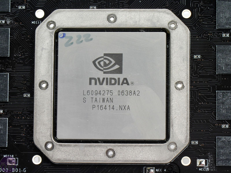
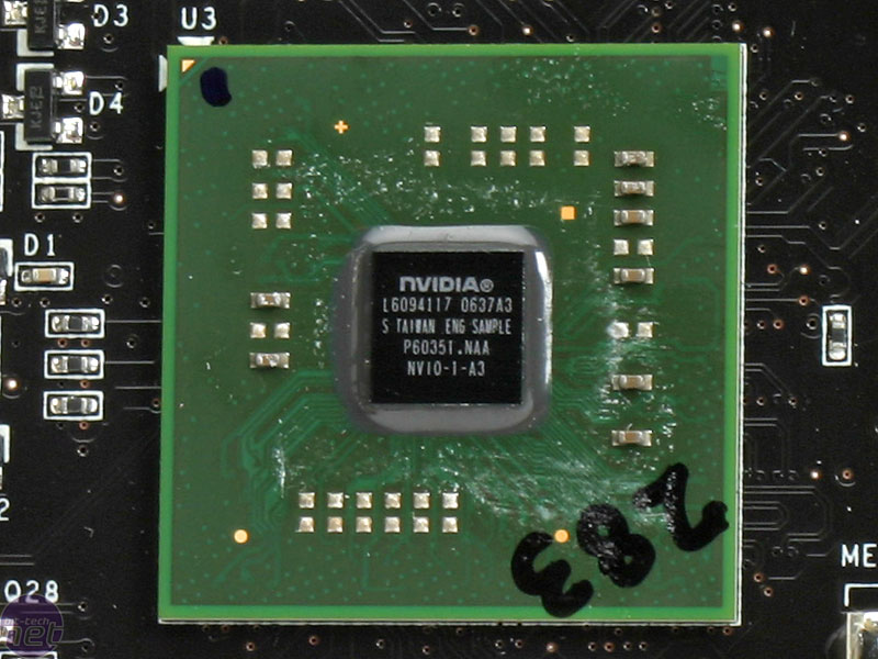
You may see the chip, and consequently the boards, get smaller next year when NVIDIA moves to shrink G80 to a 65nm process. The second chip you can see controls input/output functions and basically functions as the RAMDAC, albeit slightly more advanced. Amusingly, it's marked as NVIO, which looks a little close to NV10, the codename for the original GeForce 256. The chip comes with support for two dual-link DVI ports with HDCP support and an HDTV-Out port to round things off.
Discuss this in the forums
YouTube logo
MSI MPG Velox 100R Chassis Review

October 14 2021 | 15:04

TOP STORIES

SUGGESTED FOR YOU