NVIDIA's SLI: Part 1 - Motherboards
May 16, 2005 | 09:31

Gigabyte GA-K8NXP-SLI - The Board
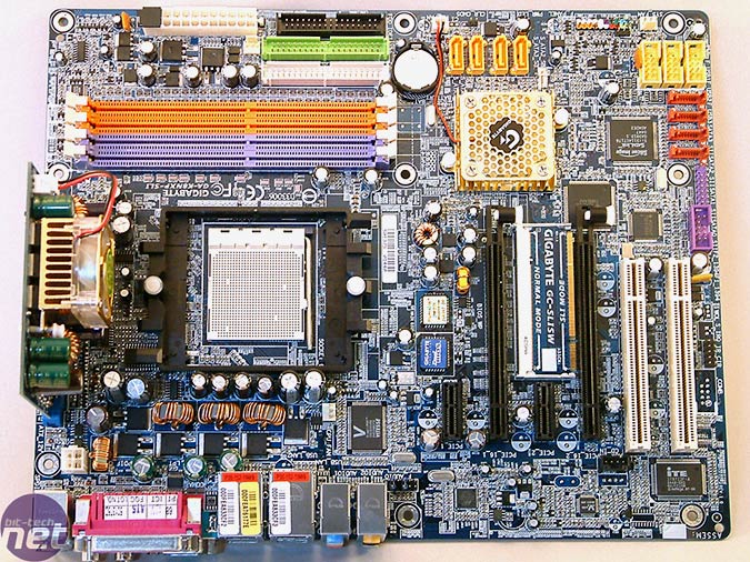
As with all of the motherboards, Gigabyte has done a good job with the general layout, but there are a few niggles that we will come to in due course. The board layout is very similar to the ASUS A8N-SLI Deluxe, with the exception of the extra space that is between the two PCI-Express x16 slots on ASUS' NForce 4 SLI implementation. Gigabyte has chosen to place the second PCI-Express x1 slot above the primary video card slot. This gives a little bit more room around the memory slots. Gigabyte's unique Dual BIOS is located directly above the left hand PCI-Express x1 slot - this allows the user to tweak to their hearts content without risk of killing the motherboard, thanks to the second 'back up' BIOS chip.
The area around the CPU socket is fairly cramped, with Gigabyte's Dual Power System (DPS) on the left hand edge of the motherboard as we look at it. The riser card was not a snug installation and we had to bend one of the capacitors out of the way slightly. The 4-pin 12v power connector is located directly below the DPS card slot. There is a line of capacitors directly below the CPU socket, up close to the heatsink retention system. With a normal heatsink/fan combination, there should be no problems with the placement of these capacitors, but with a slightly more-extravagant cooling solution, such as a vapour phase change system or water block, you may encounter installation problems. Interestingly, Gigabyte has opted not to cool the mosfets. These days, most motherboard manufacturers seem to be opting for cooling on the mosfets that regulate the CPU's voltage - we've found in the past that efficiency improves slightly with additional cooling, most definitely when overvolting the CPU during heavy overclocking.
The four DDR memory slots are located directly above the CPU socket in a two-by-two configuration. In order to enable dual channel DDR, you will need to install memory modules in adjacent memory slots, by colour. Along the top edge of the board, there is the 24-pin ATX power connector along with the IDE and floppy drive connectors. The CMOS battery is located to the right of the memory slots, while the CMOS reset jumper is located above the four SATA II ports connected to the NForce 4 MCP. The NForce 4 MCP is located below the primary PCI-Express x16 slot and is actively cooled with a low-profile heatsink/fan combination. From testing, we found that the fan was relatively quiet. In contrast, the fan on the DPS add-in card seemed to emit a little more noise than the chipset. It was not a high-pitched whine, but the noise was audible above the rest of the system.
Along the right hand edge of the board, there are three USB 2.0 headers supporting two ports each, four SATA ports controlled by the Silicon Image 3114 RAID controller and two IEEE1394 connectors that support two full sized ports and a mini port. The Silicon Image 3114 RAID controller is capable of RAID 0, 1, 0+1 and 5.
Unlike the ASUS A8N SLI and DFI LANPARTY nF4 SLI-DR, there is no additional power requirement on this motherboard - both ASUS and DFI suggest that you attach the additional 4-pin molex connector and an additional floppy connector, in the case of the DFI, to give better stability under high load.
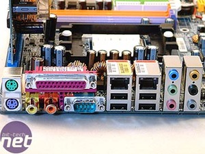
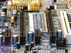
The back plate features two PS/2 ports, four USB2.0 ports, serial and parallel ports, S/PDIF RCA input and output jacks, one NVIDIA Gigabit LAN port, one Marvell Gigabit LAN port, and six analogue audio ports. The SLI controller is virtually the same design as is used on the ASUS A8N-SLI Deluxe, in the form of a 'SO-DIMM' card and slot combination. It's located in between the two PCI-Express x16 slots, and it is not quite as easy to change as it is on the A8N-SLI Deluxe.
The BIOS
The BIOS menu is a fairly standard layout, with the only major issue being the fact that you need to press CTRL+F1 in order to view the Advanced Chipset Features that are present in the BIOS. The MB Intelligent Tweaker (M.I.T.) menu is where all voltage and frequency settings are configured. The CPU front side bus clock ranges from 200MHz to 400MHz in 1MHz increments, and the PCI-Express bus is controlled separately to the front side bus. After CTRL+F1 has been pressed to activate expert mode, you are greeted with the Advanced Chipset Features menu, along with some additional features in the M.I.T menu. The Advanced Chipset Features menu gives the user the option to adjust memory and chipset related timings, including those related to the HyperTransport bus.
VCore voltage adjustment is respectable, with a maximum of 1.75v available to the CPU, while memory voltage can only be increased by a mere 0.2v over the default value. That's not ideal for the budding overclocker that is looking to keep the memory bus in sync with the CPU's front side bus. Finally, both HyperTransport and Chipset voltages can be increased by 0.3v above their default values. While these voltage adjustment ranges are not as comprehensive as the DFI LANPARTY nF4 SLI-DR, the allowable maximums should allow for some overclocking. If you're looking to push your system to the maximum, this board may not meet your requirements due to the relative lack of voltage adjustment.

As with all of the motherboards, Gigabyte has done a good job with the general layout, but there are a few niggles that we will come to in due course. The board layout is very similar to the ASUS A8N-SLI Deluxe, with the exception of the extra space that is between the two PCI-Express x16 slots on ASUS' NForce 4 SLI implementation. Gigabyte has chosen to place the second PCI-Express x1 slot above the primary video card slot. This gives a little bit more room around the memory slots. Gigabyte's unique Dual BIOS is located directly above the left hand PCI-Express x1 slot - this allows the user to tweak to their hearts content without risk of killing the motherboard, thanks to the second 'back up' BIOS chip.
The area around the CPU socket is fairly cramped, with Gigabyte's Dual Power System (DPS) on the left hand edge of the motherboard as we look at it. The riser card was not a snug installation and we had to bend one of the capacitors out of the way slightly. The 4-pin 12v power connector is located directly below the DPS card slot. There is a line of capacitors directly below the CPU socket, up close to the heatsink retention system. With a normal heatsink/fan combination, there should be no problems with the placement of these capacitors, but with a slightly more-extravagant cooling solution, such as a vapour phase change system or water block, you may encounter installation problems. Interestingly, Gigabyte has opted not to cool the mosfets. These days, most motherboard manufacturers seem to be opting for cooling on the mosfets that regulate the CPU's voltage - we've found in the past that efficiency improves slightly with additional cooling, most definitely when overvolting the CPU during heavy overclocking.
The four DDR memory slots are located directly above the CPU socket in a two-by-two configuration. In order to enable dual channel DDR, you will need to install memory modules in adjacent memory slots, by colour. Along the top edge of the board, there is the 24-pin ATX power connector along with the IDE and floppy drive connectors. The CMOS battery is located to the right of the memory slots, while the CMOS reset jumper is located above the four SATA II ports connected to the NForce 4 MCP. The NForce 4 MCP is located below the primary PCI-Express x16 slot and is actively cooled with a low-profile heatsink/fan combination. From testing, we found that the fan was relatively quiet. In contrast, the fan on the DPS add-in card seemed to emit a little more noise than the chipset. It was not a high-pitched whine, but the noise was audible above the rest of the system.
Along the right hand edge of the board, there are three USB 2.0 headers supporting two ports each, four SATA ports controlled by the Silicon Image 3114 RAID controller and two IEEE1394 connectors that support two full sized ports and a mini port. The Silicon Image 3114 RAID controller is capable of RAID 0, 1, 0+1 and 5.
Unlike the ASUS A8N SLI and DFI LANPARTY nF4 SLI-DR, there is no additional power requirement on this motherboard - both ASUS and DFI suggest that you attach the additional 4-pin molex connector and an additional floppy connector, in the case of the DFI, to give better stability under high load.


The back plate features two PS/2 ports, four USB2.0 ports, serial and parallel ports, S/PDIF RCA input and output jacks, one NVIDIA Gigabit LAN port, one Marvell Gigabit LAN port, and six analogue audio ports. The SLI controller is virtually the same design as is used on the ASUS A8N-SLI Deluxe, in the form of a 'SO-DIMM' card and slot combination. It's located in between the two PCI-Express x16 slots, and it is not quite as easy to change as it is on the A8N-SLI Deluxe.
The BIOS
The BIOS menu is a fairly standard layout, with the only major issue being the fact that you need to press CTRL+F1 in order to view the Advanced Chipset Features that are present in the BIOS. The MB Intelligent Tweaker (M.I.T.) menu is where all voltage and frequency settings are configured. The CPU front side bus clock ranges from 200MHz to 400MHz in 1MHz increments, and the PCI-Express bus is controlled separately to the front side bus. After CTRL+F1 has been pressed to activate expert mode, you are greeted with the Advanced Chipset Features menu, along with some additional features in the M.I.T menu. The Advanced Chipset Features menu gives the user the option to adjust memory and chipset related timings, including those related to the HyperTransport bus.
VCore voltage adjustment is respectable, with a maximum of 1.75v available to the CPU, while memory voltage can only be increased by a mere 0.2v over the default value. That's not ideal for the budding overclocker that is looking to keep the memory bus in sync with the CPU's front side bus. Finally, both HyperTransport and Chipset voltages can be increased by 0.3v above their default values. While these voltage adjustment ranges are not as comprehensive as the DFI LANPARTY nF4 SLI-DR, the allowable maximums should allow for some overclocking. If you're looking to push your system to the maximum, this board may not meet your requirements due to the relative lack of voltage adjustment.

MSI MPG Velox 100R Chassis Review
October 14 2021 | 15:04


Want to comment? Please log in.