Inno3D nForce 680i SLI
February 17, 2007 | 10:05
Companies: #inno3d #innovision #intel #nvidia #test

Board Layout (continued)
Dual Gigabit Ethernet is the standard these days, although consumer gigabit switches and routers are still lagging behind (like PCI-Express x1 cards?) or seriously expensive. If you're sending high-definition content or serving a few people videos over LAN you'll want gigabit, so at least having it on the motherboard makes a partial investment already. Also, given the fact that NVIDIA’s integrated PHY Ethernet and TCP/IP offloading frees up the CPU to do other things; this allows you to serve other people’s data while playing games and should result in a minimal impact on performance.The onboard power and reset switches are a godsend for tweakers and overclockers who play with the board outside on the desktop, but Inno3D has committed the sin of soldering a PC speaker right to the board itself.
This is this a complete pain in the posterior; some programs or the BIOS will insist on using it even if you turn it off, and you know it'll blare out at the most inconvenient time (usually in those frustrating 2am “I must fix this” sessions when everyone else is asleep). Considering the board includes an LED hex readout to diagnose BIOS problems I can't see why you'd need one. A better solution would be to wire up the BIOS to use the onboard audio which has significantly more fidelity and can be turned off.
Generally all the space has been used well, and it is maxed it out with seven expansion slots, including two PCI-Express x1 and two PCI slots, one of which is still usable when using a pair of dual slot cards in SLI.
Rear I/O
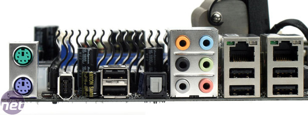
Even though there is optical S/PDIF out, there’s no optical in, coaxial in or coaxial out on the rear I/O panel. However, there are pin outs on the board for S/PDIF in the bottom corner, although there is nothing in the box to make use of them. If you're after legacy ports then still provided is a serial port pin out, but again nothing is in the box to make use of it.
BIOS
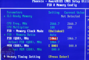
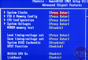
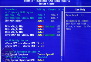
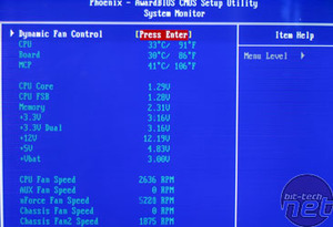
Frequency Adjustments:
PCI-Express x16 slots (100-200MHz in 1MHz increments); SPP-MCP Hyper Transport (200-500MHz in 1MHz increments); HyperTransport multiplier (1-5x); Front Side Bus (QDR - 400-2500MHz in 1MHz increments); Memory (DDR - 400-1400MHz in 1MHz increments);
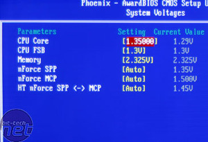
Voltage Adjustments:
CPU Core (0.5V to 1.8V in 0.00325V increments); CPU FSB (1.2V to 1.5V in 0.1V increments); Memory (1.8V to 2.5V in 0.025V increments); Northbridge (1.5V to 1.7V in 0.025V increments); Southbridge (1.5V to 1.75V in 0.25V increments); HyperTransport (1.2V to 1.55V in 0.05V increments);
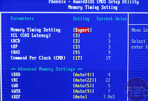
Memory Timings:
CAS Latency (tCL), RAS to CAS Delay tRCD, RAS to CAS Delay tRP, RAS Cycle Time (tRAS), Command Rate, Row Active to Row Active Delay (tRRD), Row Cycle Time (tRC), Write to Read Time (tWR), Internal Write to Read Command Delay (tWTR), Time between RAM refreshes (tREF).
The memory timings are not massively comprehensive but the essential adjustments are supported. The same goes for the voltages: while digital PWMs would give you more and finer adjustments, what's necessary is included, even to a liberal degree with CPU up to 1.8V and memory to 2.5V.

MSI MPG Velox 100R Chassis Review
October 14 2021 | 15:04


Want to comment? Please log in.