Due to the fact that raw memory speed has never really been able to keep up with CPU performance, memory system designers have always used multi-factored improvements. For economic reasons, the key objective has always been to keep the manufacturing cost as low as possible.
Instead of relying on improving raw memory speed which would be more expensive, the innovative designers created many parallel accesses methods to compensate for slower speed increments. These include the creation of all of the above: Double-Data Rate technology, Dual or Quad Channel modes, and Pre-fetching technology, among others.
It is important to note that there are fundamental engineering cost constraints with DDR DRAM technology that limits the core performance to 200MHz. Increasing the bus efficiency via higher operational frequency is much easier than raising DRAM core frequency.
Design and manufacturing breakthroughs in accurate signal management and Electromagnetic Interference (EMI) control mechanisms are compulsory on the motherboard and memory module. Hence, memory improvement is not solely a matter of consideration for DRAM designers, but a coordinated industry wide effort from the CPU architects, chipset and DRAM designers to the motherboard and memory module manufacturers.
Intel has already released first generation DDR3 motherboards under the “Bearlake” 3-series family this year in the form of the P35 and X38 chipsets. Future chipset from Nvidia and later AMD, for its own CPUs, will also support DDR3 in 2008. Current DDR2/DDR3 "combo" boards are capable of supporting existing DDR2-800 or the new DDR3-1066/1333 memory modules, but not both standards at the same time. DDR2 and DDR3 use different memory slots as they have distinctive module key-notch location.

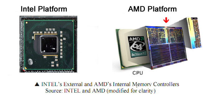
AMD is only the main processor manufacturer with a memory controller built into the CPU, and has done since the Athlon 64 was launched three years ago. Intel is due to follow this trend in late 2008 with its new "Nehalem" core. AMD will support its third generation HyperTransport technology, along with a new CPU socket, codenamed AM2+, later this month. AMD support for DDR3 technology will come in the form of AM3 socket and from the 45nm Deneb, Propus and Regor cores sometime in 2008, according to road maps.
Interestingly, with AMD going back to the doctrine of processor-socket backward compatibility, we expect these 45nm cores to be compatible with its generation previous to it.
The immediate economic benefit of integrating the memory into the CPU package is the reduction in manufacturing cost of the motherboard for that particular platform. The technological benefit is the removal of a stage from the line of data transfer. Integrating the memory controller removes the need for a physical Front Side Bus (FSB). This makes the design and testing process for mainboard manufacturers simpler by placing the burden solely on CPU designers - there's less EMI issues and the whole system has an inherently lower power design. In theory this arrangement could improve memory performance fairly significantly by eliminating incidents of bandwidth bottleneck around the Front Side Bus.
The down side of integrated memory controller is that it takes up space on the processor die which can potentially be used for more L1, L2 and L3 cache. You're also limited by the performance of the single memory controller only, instead of having a choice of chipset like with Intel systems. In addition, any Direct Memory Access (DMA) has to go through the CPU before getting to memory in an AMD system, creating an extra latency negotiation for other component parts like graphics cards which require fast access.
Instead of relying on improving raw memory speed which would be more expensive, the innovative designers created many parallel accesses methods to compensate for slower speed increments. These include the creation of all of the above: Double-Data Rate technology, Dual or Quad Channel modes, and Pre-fetching technology, among others.
It is important to note that there are fundamental engineering cost constraints with DDR DRAM technology that limits the core performance to 200MHz. Increasing the bus efficiency via higher operational frequency is much easier than raising DRAM core frequency.
Design and manufacturing breakthroughs in accurate signal management and Electromagnetic Interference (EMI) control mechanisms are compulsory on the motherboard and memory module. Hence, memory improvement is not solely a matter of consideration for DRAM designers, but a coordinated industry wide effort from the CPU architects, chipset and DRAM designers to the motherboard and memory module manufacturers.
Memory Controllers
The responsibility of the memory controller is to command, manage and route signals to and from the memory modules. Each DRAM usually has four or eight memory banks that are accessed in a similar way to a Microsoft Excel worksheet: with rows and columns. Whenever the CPU needs read or store data, it sends the information to the RAM via the memory controller.Intel has already released first generation DDR3 motherboards under the “Bearlake” 3-series family this year in the form of the P35 and X38 chipsets. Future chipset from Nvidia and later AMD, for its own CPUs, will also support DDR3 in 2008. Current DDR2/DDR3 "combo" boards are capable of supporting existing DDR2-800 or the new DDR3-1066/1333 memory modules, but not both standards at the same time. DDR2 and DDR3 use different memory slots as they have distinctive module key-notch location.

AMD is only the main processor manufacturer with a memory controller built into the CPU, and has done since the Athlon 64 was launched three years ago. Intel is due to follow this trend in late 2008 with its new "Nehalem" core. AMD will support its third generation HyperTransport technology, along with a new CPU socket, codenamed AM2+, later this month. AMD support for DDR3 technology will come in the form of AM3 socket and from the 45nm Deneb, Propus and Regor cores sometime in 2008, according to road maps.
Interestingly, with AMD going back to the doctrine of processor-socket backward compatibility, we expect these 45nm cores to be compatible with its generation previous to it.
The immediate economic benefit of integrating the memory into the CPU package is the reduction in manufacturing cost of the motherboard for that particular platform. The technological benefit is the removal of a stage from the line of data transfer. Integrating the memory controller removes the need for a physical Front Side Bus (FSB). This makes the design and testing process for mainboard manufacturers simpler by placing the burden solely on CPU designers - there's less EMI issues and the whole system has an inherently lower power design. In theory this arrangement could improve memory performance fairly significantly by eliminating incidents of bandwidth bottleneck around the Front Side Bus.
The down side of integrated memory controller is that it takes up space on the processor die which can potentially be used for more L1, L2 and L3 cache. You're also limited by the performance of the single memory controller only, instead of having a choice of chipset like with Intel systems. In addition, any Direct Memory Access (DMA) has to go through the CPU before getting to memory in an AMD system, creating an extra latency negotiation for other component parts like graphics cards which require fast access.

MSI MPG Velox 100R Chassis Review
October 14 2021 | 15:04


Want to comment? Please log in.