Latencies
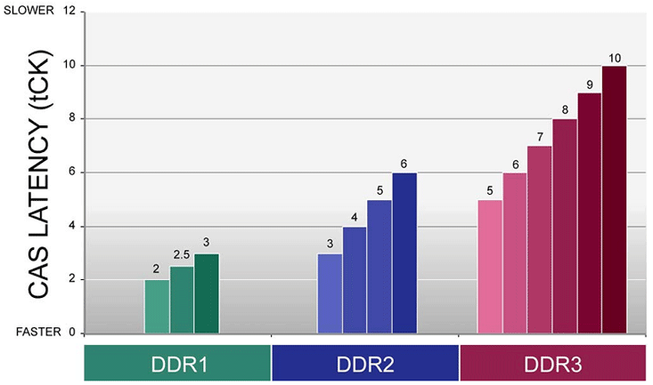
Each progression of DDR generation allows for higher capacity at faster data rate, but the trade-off is decreasing stability and signal accuracy. Therefore, each generation of DDR needs to accommodate faster frequency with higher signal latencies.Latency is regarded as a Pause or Delay in time. When there are changes in DDR signaling commands, the memory subsystems need to pause between different memory commands. It is like a train moving into a station and stopping for unloading and loading of passengers.
There are many types of latencies. CAS Latency is often regarded as one of the most important, however as generations of DDR memory progress it alone becomes less critical in preference to a combination of several latency values. Many memory modules denote CAS Latency as either “CL" or simply “C”. So, memory modules with CAS Latency of 3 clock cycles are usually marketed as a CL3 or C3. Optimisation on this subject will be discussed in a later article.

Evolutionary Progress
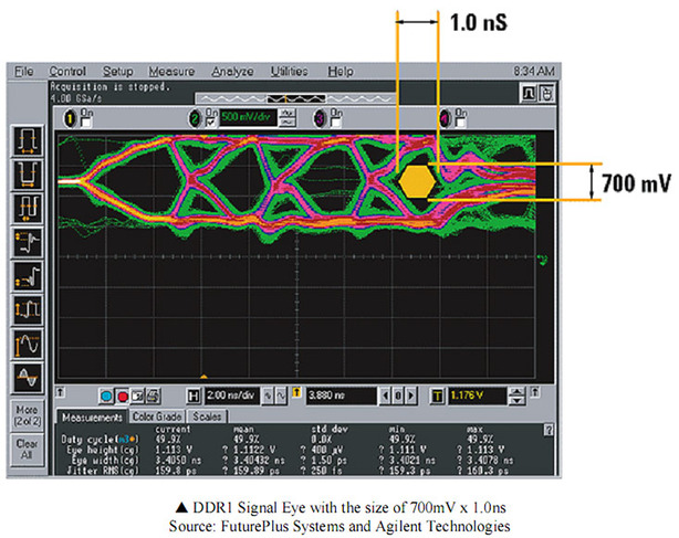
Driven by the requirement for higher data throughput, various technologies involved in DDR went through a series of evolutionary steps, while maintaining as economic to make as possible.Two of the challenges faced with increasing the memory frequency for data transfer are signal noise level and timing accuracy. This is often related as the Valid Data Window (DVW). Valid Data Window is sometimes called Data-Valid Window (just to confuse things) or simply the “Data Eye”. It is the primary factor used to determine the level of signal reliability.

Various noise termination schemes have been used. For example: DDR1 uses motherboard resistive termination method, followed by On-Die Termination (ODT) in DDR2. DDR3 takes ODT further by allowing for dynamically adjusting ODT values according to the situation. When combined with various signal calibration techniques, data integrity can be managed reasonably well for a faster transfer rate. All memory modules and motherboards are required to be tested and validated for signalling accuracy during design and post-assembly in order for the various built-in calibration schemes to function properly.
To achieve higher efficiency and lower heat dissipation, memory voltage is required to fall. Data-centre owners, desktop and notebook consumers are becoming more interested in low power computers for reasons including being more environmental, longer mobile computing time and a general reduction in operational costs.
Modern data centres utilize huge amount of air conditioning to maintain operation. For example, LucasFilm’s data centre uses 25 tons of coolant in 32 air conditioning units to keep their systems running. Power efficiency is usually calculated in terms of performance per watt so any reduction in wattage for the same performance is a boon for the industry.
Memory systems in computers do not make major paradigm shifts without many years of advance planning and industry wide consultations. Revisions after revisions are submitted by members to a design governing body like JEDEC and a committee of partners will oversee the whole design and ratification process.
The exorbitant cost of the fabrication and testing equipment involved in the manufacturing process is a significant inhibitive inertia for change as Automatic Test Equipment (ATE) is extremely expensive and usually cost millions of dollars per unit. According to, Brad Snoulten, from MOSAID Systems, the two main challenges are:
- Memory manufacturers cannot afford to purchase or replace multiple million-dollar testers to address advancing production or engineering test needs.
- Memory ATE vendors are tasked with the challenge of designing affordable solutions with protection against long-term obsolescence. These problems are exacerbated by the volatility of eroding memory margins and ever increasing device complexity.

MSI MPG Velox 100R Chassis Review
October 14 2021 | 15:04


Want to comment? Please log in.