
DRAM Packaging
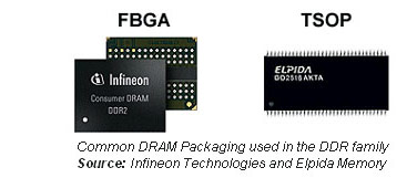
Memory chip packaging designs changed significantly when the industry moved from SDR to DDR. Some common DRAM packaging includes Thin Small-Outline Package (TSOP), Chip-Scale Packaging (CSP), Low-Profile Quad Flat Pack (LQFP) and Ball Grid Array (BGA).The most common packaging used in DDR includes variations of either BGA or TSOP, of which, TSOP is more commonly used in DDR1 whereas current DDR2 and DDR3 standards utilize FBGA, with only minor variations between DRAM manufacturers.
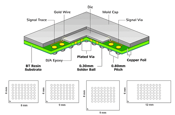
Sample of FBGA with different Form Factors
Source: Spansion Memory (modified for clarity)
The main advantages of FBGA include high density, better heat dissipation and shorter connectors resulting in fewer signal distortions. FBGA should not be confused with Fortified BGA, which is explained at the bottom of the page.
BGA-PCB Joints Stress
On the other hand, shorter connectors arranged in a grid fashion at the bottom of the chip can result in non-uniform stress between each pin or solder ball during thermal expansion and contraction cycles. This happens when the DRAM heats up and expands at a different rate relative to the attached Printed Circuit Board (PCB).The different rate of expansion between the PCB and the DRAM chip stresses the soldered balls and can result in fractured connections - this is one of the reasons why users should not increase the DRAM voltage higher than the specification, unless there is extra effort applied to keeping the memory cool. Higher voltage will generate more heat and degrade the internal DRAM circuitries at a faster rate.
Certain memory modules by OCZ (FlexXLC, Reaper, ReaperX) and Corsair (DHX, Dominator) have advanced thermal technology that reduces the discrepancy between DRAM and PCB during thermal cycles.
The way OCZ and Corsair confirm the effectiveness of their PCB heat transfer technology is by stressing their modules to extreme temperature cycles for long period, and then inspect the DRAM ball connections for fractures with X-ray. This is an extremely time consuming process and one of the important points for overclockers to keep in mind.
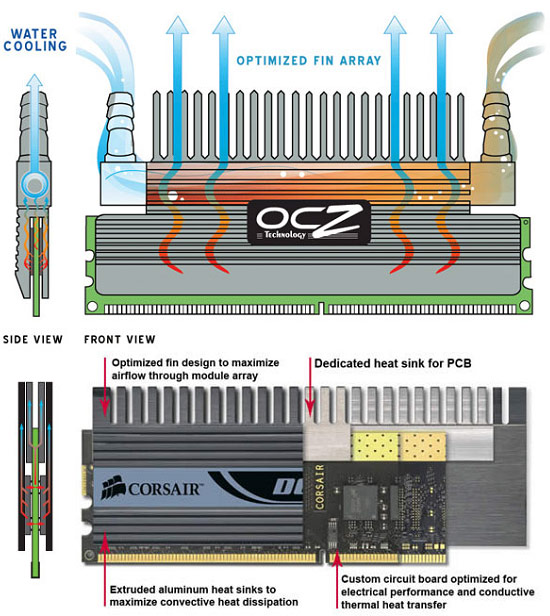
specialised PCB cooling for FBGA DRAM from OCZ and Corsair
Source: OCZ Technology and Corsair Memory
As previously mentioned, another variation of BGA technology is known as Fortified-BGA. Like the name implies, it improves DRAM reliability during thermal cycles (from hot to cold, vice versa) by fortifying the connecting points. Solder ball diameter at the bottom of the DRAM chip is directly proportional to solder joint reliability during temperature cycles. The large the diameter, the more reliable it will be – this is one of the reasons why certain memory modules can tolerate higher temperature.
RELATED ARTICLES


MSI MPG Velox 100R Chassis Review
October 14 2021 | 15:04

Want to comment? Please log in.