DRAM fabrication
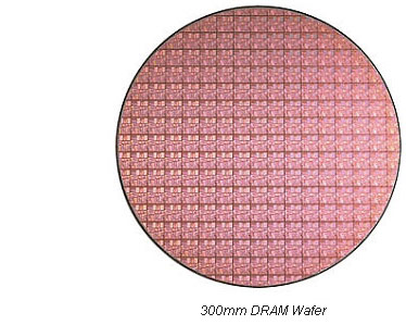
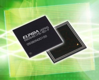
Each memory chip packaging consists of one or more dies where each die was cut from a larger circular piece of silicon wafer. Vigorous inspections are done during manufacture to make sure they are flawless. Once individual dies have been cut, they are placed into a package and the connections are bonded – this forms the basis of the DRAM chip.
An important aspect in DRAM manufacturing is the wafer fabrication resolution, which is measured in nanometres. Like the evolution of CPU, DRAM technology follows a steady path of miniaturisation to achieve higher density and greater performance.
DRAM performance is tied to key technological progress in the lithographical fabrication process, these advancements are like exclamation points in the DRAM evolutionary time line. The table below illustrates the targets of DRAM manufacturing process set by The International Technology Roadmap for Semiconductors (ITRS).

ITRS’s DRAM Targets
Source: Semiconductor Industry Association
ITRS explains, “The DRAM half pitch correlates to the width, and space in between metal lines connecting DRAM bit cells – the smaller the half pitch, the more DRAM bit cells can fit in a given area. ...The shorter the gate length, the faster the switch time becomes.”
Creating smaller circuits allows the signals to travel faster while using less power. Each stage of advancement will see an increase in efficiency, larger capacity and general improvement in performance characteristics: this is very similar to the evolution of CPU technology.
Major changes are expected in 2010 and 2011 as the industry moves into 45nm fabrication, 450mm wafer, 45 micro metre wafer thickness and 3D chip packaging technology. There are many concerns made by companies when technology goes through a paradigm shifts, mostly related to the costs of equipment replacement or retooling, and the degradation of electrical properties in some materials at 45nm or smaller.
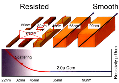
As the industry moves into 45nm and beyond, there will be more electrical resistances and electronic scattering effects. As circuitry dimension is reduced, electricity has more trouble flowing because of greater resistance in the smaller copper wiring, raising the risk of defects or compromising signal integrity.

ITRS’s DRAM Targets
Source: Lecture by Dr. Tsujimura - ITPC Panelist (modified for clarity)
In addition to improving the ‘interconnect’ wiring conductivity, another interesting way to improve current flow is to reduce the transistor resistive nature. Manufacturers use advanced material science to improve the fundamental die circuitries and in 2007, Toshiba was able to get 35 percent higher current flow from a transistor by using a different material configuration and dispersing doping agents in the boundary surface between the transistor electrodes and silicon substrate.
There has also been some basic research into using Carbon Nanotubes (CNT) as the fundamental circuitries and interconnects. It is regarded as one of the promising elements in sustaining Moore’s Law well into 2020. According to, Philip G. Collins, and, Phaedon Avouris, in Scientific American (December 2000 issue), metallic nanotubes can have an electrical current density more than 1,000 times greater than metals such as silver and copper.
Using Carbon Nanotubes is challenging on a few fronts for starters, the fabrication and circuitry layout processes are extremely complicated. Various manufacturing techniques have considered including print-on and growth approaches, but both are still extremely young and don't yet directly relate to the application in mass production of semiconductors.
In May 2007, Micron Technology announced the availability of DDR2 and DDR3 DRAM chips using the 78-nanometre process. With this new fabrication process, Micron was able to increase the data frequency to 1,066MHz while keeping the operational voltage at the common 1.8v. This is a significant achievement because it makes the DDR2 1,066MHz memory highly compatible with all motherboards by operating at JEDEC approved DDR2 voltage standard, meaning it also readily complies with AMD’s new AM2+ CPUs that operate at 1,066MHz DDR2 memory speed.
Modules built with these ICs will also have more margins to overclock, as is seen in Micron’s current "6F2" die DDR3 die offerings; "By using a 78 nm process and 6F2 technology, Micron achieves the smallest cell size of any DRAM device analysed to date at only 0.0365 µm... the metal-insulator-metal (MIM) capacitor cell design and recessed-channel access transistor provide small wordline and bitline pitch measurements of 156 nm each." Currently, all performance DDR3 at low latency 1,333MHz and 1,600MHz and above use Micron D9-based memory chips.
This is the key reason why the core enthusiasts and overclockers seek out specific DRAM chips and track them down to the particular memory brand and model – this has also previously been the case with Winbond BH-5 and Samsung TCCD chips used on some DDR1 modules. It is important to note that some manufacturers like Corsair and OCZ Technology will tend to pre-overclock these quality DRAMs that are rated at slower frequencies, to perform at faster clock speeds by increasing operational voltage.
According to a report by Nikkei Business Daily, Japanese scientists and engineers at New Energy and Industrial Technology Development Organization (NEDO) have successfully created a 26-nanometre design by using Extreme Ultraviolet (EUV). The EUV system was developed by Canon and a mass production system will most likely be available at the earliest in 2011, but more likely in 2012.
That's all for Part 2 - In the next chapter we investigate the specific details of DDR, DDR2 and DDR3 technology!

MSI MPG Velox 100R Chassis Review
October 14 2021 | 15:04


Want to comment? Please log in.