Foreword
by Richard SwinburneRyan Leng is an independent technology consultant and auditor for corporations in computer systems involving hardware, software, networking, security, IT policy formulation and training.
Originally trained in Computer Science and Economics, he has since worked in many fields relating to computer hardware integration, software design and engineering, surveillance systems, advertising, multimedia production, user-Interface engineering and graphic designs.
Ryan approached bit-tech with his unpublished book on DDR technology a short while ago, and when we read it we were greatly impressed with the depth and attention to detail, as well as being able to convey complex ideas in an easy to understand manner.
Whether you are adept in the knowledge of memory technology, it’s still an interesting read for a fundamental part of the PC’s architecture. We’ve cut his work up into several parts and this is the third article in the series.
For those that didn’t read Ryan’s first two articles on memory technology we highly recommend that you do, but don't fret if you haven't got the time to read them, because you don't need them to enjoy today's material.
The Revolutionary Change from Asynchronous and Synchronous Clocks
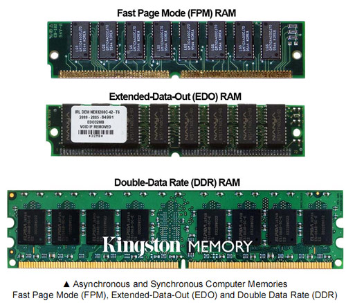
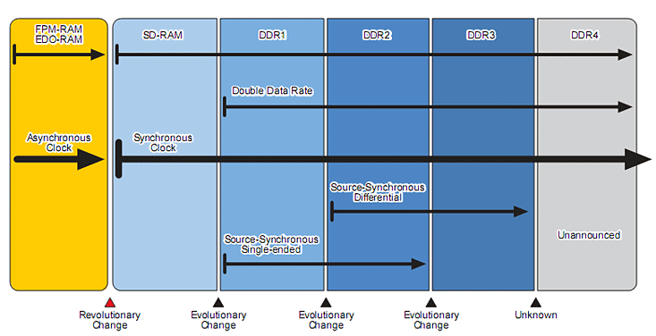
Earlier generations of memory technology were based on asynchronous clock architectures. Asynchronous memories include Fast Page Mode (FPM) RAM, Extended-Data-Out (EDO) RAM and other variants. As the name implies, the memory is not tied or synchronized to the system bus clock, and as such, this design has fundamental limitations that prevented the bus from performing faster than 66MHz.The move from asynchronous to synchronous clock dependent memory was "a revolutionary change, [where] the signalling totally changed..." according to Brett Williams, Senior Marketing Manager in Computing at Micron Technology.

Modern computer memory still relies on a synchronous clock design which became prominent after mass market adoption of Synchronous Dynamic RAM, or SD-RAM, that began at 66MHz with a limitation of one signal per clock cycle. This was evolved into DDR memory, or Double Data Rate Synchronous Dynamic Random Access Memory, which was a class of SD-RAM that was designed to perform better by efficiently attaching two data signals to a single clock cycle.

It is important to recognize at this point that what we call “The Computer Memory” is in fact an inseparable group of sub-systems ranging from RAM modules, the motherboard, its MCH or Memory Controller Hub, and the CPU. We know that sometimes the CPU integrates the MCH into its design, like with AMD’s Athlon 64 and Phenom processors.

MSI MPG Velox 100R Chassis Review
October 14 2021 | 15:04


Want to comment? Please log in.