The First Generation: DDR1
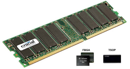
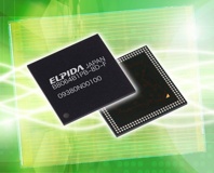
The first generation of the desktop-based Double-Data Rate (DDR1) memory module was designed with 184-pin interface, up from the 164-pin used with SD-RAM. DDR1 is commonly based on Thin Small-Outline Package (TSOP) chips, and while some Ball Grid Array (BGA) based DRAM were used but very rare. You can read more about packaging technologies in Part two of this series.
The downside of TSOP chips is that it requires more PCB real estate where the connectors extrudes from the sides – this means lower density or specially designed modules for low height and mobile solutions. TSOP also demonstrates some signalling weaknesses at higher speed in comparison to BGA.

DDR1 DRAM often has a maximum operating temperature around 85˚C/185˚F, but it can sometimes be lower depending on the specific part and manufacturer. Theoretically, DDR1 modules with TSOP chips could withstand larger degree of temperature cycles without fracturing the connecting pins when compared to BGA based DRAM found in DDR2 and DDR3 because the solder points are larger and easier to apply.
A memory module’s maximum operating temperature is always much lower than DRAM’s specification but this factor varies between manufacturers of memory chips and printed circuit boards (PCBs) as well as thermal management solutions employed.
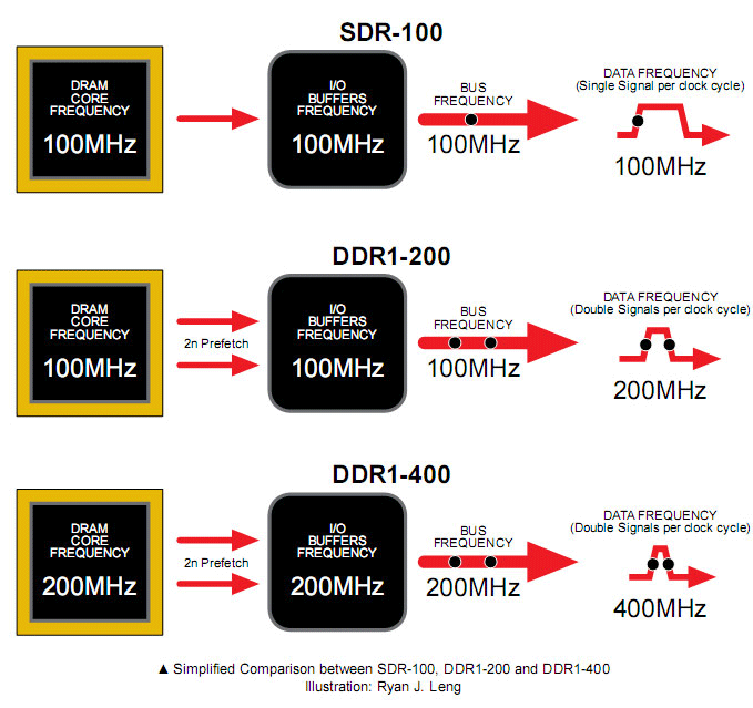
Official DDR1 bus frequencies are commonly 100MHz, 133MHz, 166MHz and 200MHz, but occasionally 150MHz, 183MHz and in excess of 200MHz has been sold to end users. Due to the fact that DDR can attach two signals per clock cycle, the standard theoretical data frequencies are 200MHz, 266MHz, 333MHz and 400MHz respectively.

DDR1 power is standardized to use 2.5V by JEDEC, however, some manufacturers certified their modules to perform at up to 2.8V+ while still remaining within their warranty coverage. This extra overhead and purchase security is handy for enthusiasts when overclocking the system.

MSI MPG Velox 100R Chassis Review
October 14 2021 | 15:04


Want to comment? Please log in.