Symmetrical T-Branch Topology
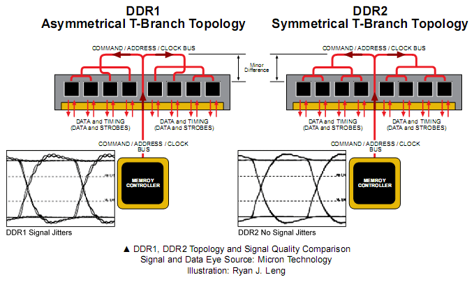
DDR2 shares a similar architecture with DDR1, known as T-Branch topology. However, DDR2 differs from the previous generation with the use of a symmetrical design. As a result, the Command, Address and Clock bus to each DRAM chip is fully proportioned improving the signal quality at higher frequencies since better symmetry reduces the signal jitter.This design is a major improvement in the ability to reduce non-monotonic signal behaviour commonly found in SDR and DDR1 bus topologies.
DDR2 T-Branch can still cause timing skew between the longer Command-Address-Clock bus and the shorter Data bus. This is because the Command-Address-Clock T-Branch bus has multiple stubs and compared to the direct nature of the Data bus. This is not a major problem under DDR2 but has been revised for DDR3 speed grades.

Data Prefetch
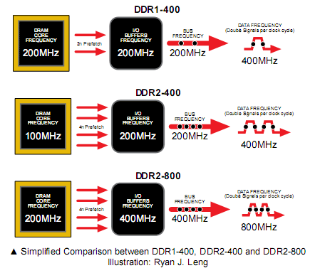
DDR2 uses a “4n-prefetch” design as opposed to DDR1’s “2n-prefetch”. At each cycle, it is able to line-up 4-bits of data from internal memory banks into IO buffers before transmitting them out on the data bus.
According to Joe Macri—a member of JEDEC DRAM committee and formerly of ATI Technologies, now AMD—the key purpose of 4n-Prefetch architecture is to decrease the DRAM core frequency relative to the need of supporting higher data rates. Thus, allowing the DRAM core to run at a quarter of the data bus frequency.
The immediate benefit of this design is the ability to maintain a relatively established manufacturing process without major re-tooling. It eases the production ramp-up and yield pressure of DDR2 chips, especially those with higher data rate and density.

MSI MPG Velox 100R Chassis Review
October 14 2021 | 15:04


Want to comment? Please log in.