
Clock Skew in Synchronous Memory
When an increasing number of circuits are synchronised to a clock, a clock delay phenomena can happen. As a result, all the data has trouble associating with the right clock and turning up on time: this phenomenon is commonly known as Clock Skew.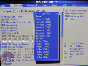
The "AI Clock Skew" option in the Asus P5E3 Premium BIOS – click to enlarge
Clock Skew can be caused by many factors including extended path, temperature fluctuation, adding multiple logic circuits along that line, material imperfections and fundamental design flaws on the motherboard – in other words, it can happen in many different parts of the memory system. De-skewing logics at different locations will try to minimise the negative effects in order to maintain a coherent relationship between the Data and the System Clock. However, as the memory performs at an ever increasing rate, not all problems can be resolved easily.
Enthusiasts may be more familiar with the appropriately named “Clock Skew” variable in the motherboard BIOS, where it can be used to attain higher level of stability when overclocking the computer memory in order to resolve Clock Skew between DIMMs. Inevitably, the faster the memory performs, the greater the probability of Clock Skew.
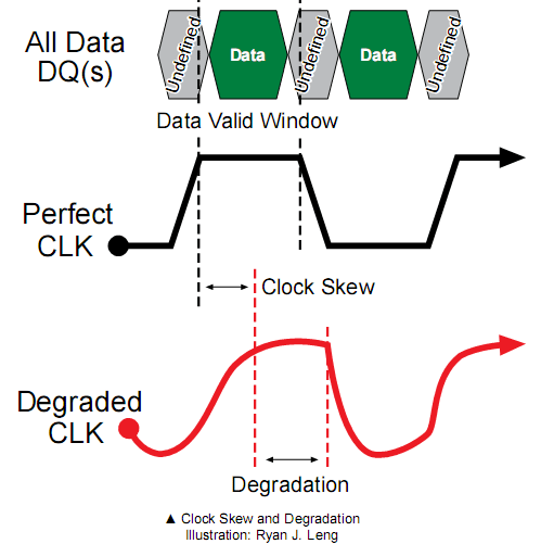
The Clock Skew can be more profound when using four memory modules instead of two in your motherboard and the skew amount depends on which two slots are being used at any one time, and the fundamental design of the PCB.
Motherboards that have gone through extensive design simulation and testing phase to attain a particularly high quality tend to manage Clock Skew issues fairly well. However, due to extremely competitive market pressure and falling product shelf-lives, many deficient motherboards are launched prematurely and hyped without having sufficient testing time, then later patched as much as possible in BIOS updates. Increasingly complex motherboard chipsets and higher memory speed are adding more opportunity of failures in this respect.
Single-ended to Differential Strobes Architecture
While the single-ended data strobe was first used in DDR1, DDR2 was the evolutionary transition point supporting both Single-ended and Differential Strobe designs. In the most basic explanation, the Single-ended Strobe relies on one oscillating wave, while Differential architecture uses two opposing oscillating waves that weave and crisscross each other.Aaron Boehm of Micron Technology stressed that “Differential clock and strobe schemes are much less sensitive to variations due to cross talk” and where it is a crucial to use the Differential design for high speed DDR2 and DDR3, Boehm explains, “as we continue to lower the voltages on the DRAM and continue to increase the speed, it is very important that the clock and strobes are less sensitive to these kinds of noise.”
With a Single-ended Strobe design, any small amount of noise and interference will skew the strobe to the left or right along the horizontal voltage threshold, which is sometimes known as the Reference Voltage level. This horizontal shift is detrimental because it represents a change in time representing a timing inaccuracy.
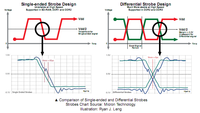
The memory relies on the stability of the ‘intersecting’ reference point to be able to read or write reliably. The Differential Strobes design is much more stable because waveform anomalies will only cause the intercepting centre point to shift up and down, representing a change in the Reference Voltage (Vdd/2), rather than a timing skewing (left or right). A fluctuating Voltage Threshold is less severe than a skew in time.
In a synchronous memory system, any significant skew in time is fatal because it means the data is no longer coherent with the clock so high speed memory will not function without the use of this Differential Signalling architecture.

MSI MPG Velox 100R Chassis Review
October 14 2021 | 15:04



Want to comment? Please log in.