Off-Chip Driver (OCD) Calibration
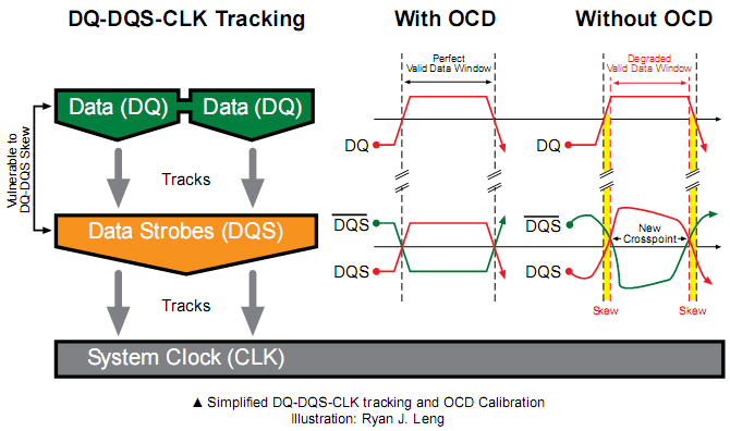
DDR2 uses Off-Chip Driver calibration to improve the tracking accuracy between the Data and the Data Strobes. The OCD calibration circuit is used to set the driver’s impedance and voltage levels for DDR2 during the memory initialization process. It is significant for the following reasons:- OCD improves signal quality by minimising Data Strobe (DQS) to Data (DQ) skews.
- It enhances signal quality by minimising Overshooting and Undershooting problems.
- It absorbs process variations from each DRAM supplier by IO driver voltage calibration.

In order to detect the best memory setting, the system sends multiple test signals based on different but pre-determined configuration values. After test completion, the value that provides the best signal quality will be used. The best DQS waveform gives the largest Data Eye area with minimal jitters, overshoot and undershoot. When properly tuned and activated, it can expand the system timing margin and therefore help to improve the overall signal characteristics.
JEDEC’s DDR2 specification documents state that if OCD calibration is not used, default parameters will be adopted during the power-up and initialisation process. Some manufacturers do not regard this as a necessary feature for DDR2 and is often left to default in order to save design costs and time. It is possible that this may be a contributing factor that causes some DDR2 800MHz (and faster) memory problems.
Drive Performance/Drive Strength and Transition Time
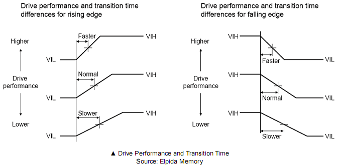
The relationship between Drive Performance and Transition Time is directly proportional. When the drive performance is set higher, the transition time between low and high voltage states of the memory becomes shorter (or faster). Drive Performance is sometimes known as “Drive Strength” or “Edge Rate”.
A signal can only be read properly when the voltage rise or fall is set between a certain level and the Transition Time is the duration required for a change from either low voltage (VIL) to high voltage (VIH) states, or vice versa. So the faster the transition time, the quicker the voltage will rise and fall.

A DFI BIOS with Drive Strength options
Stronger Drive Performance will ramp up the voltage more quickly for the rising part of the wave. Inversely, it will force a faster voltage decrease on the falling part of the wave. It is important to note that the Drive Performance function is used in many areas and generally, the concept is fairly universal but should not be confused as representation of a single factor in a particular device or area.
In some motherboards, there are many aspects of the memory subsystems where the user can change various Drive Strength values. Setting the Drive Performance too strong can have destructive overshooting and undershooting effects, thus jeopardising the data integrity as much as setting it to low.

MSI MPG Velox 100R Chassis Review
October 14 2021 | 15:04


Want to comment? Please log in.