The Fly-by Topology
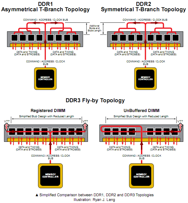
For better signal quality at higher speed grades, DDR3 adopts a so called “Fly-by” architecture for the commands, addresses and clock signals. This effectively reduced the number of stubs and signalling length from the DDR2 T-Branch architecture to a more elegant and straightforward design.The Fly-by topology generally connects the DRAM chips on the memory module in a series, and at the end of the linear connection is a grounded termination point that absorbs residual signals, to prevent them from being reflected back along the bus.
We recently asked Aaron Boehm, an Application Engineer at Micron about how important the Fly-by topology is to DDR3. He said that the Fly-by design was “very important in DDR3. Probably one of the biggest advantages of moving to the Fly-by topology is that we are able to achieve a much faster slew rate for the signal. This gives us a bigger data-eye, which is very important in DRAM.”
Boehm stressed that “DDR3 will not be able to signal without [the Fly-by design].” This new architecture was implemented to avoid DDR2’s T-Branch limitations at higher speed, because “the addressing commands all have to get to the DRAM in one clock interval. The Fly-by topology was able to get around this. If you start to increase your speed, getting those signals to the DRAM in one interval is pretty tough.”

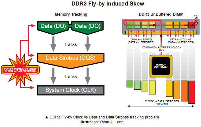
Despite the advantages of the Fly-by topology, there is an added complexity; the sequential Fly-by connection of the Command-Address-Clock bus to the DRAMs will cause increasing Clock Skew with the Data bus at every DRAM down the line. In short, the Command-Address-Clock bus signals travel down the line with increasing delay.

MSI MPG Velox 100R Chassis Review
October 14 2021 | 15:04


Want to comment? Please log in.