Board Layout and Detail Continued
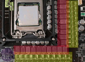
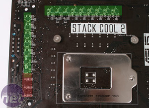
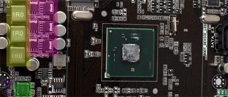
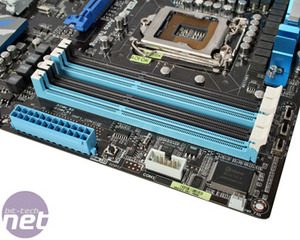
The CPU socket gets 16 phases consisting of a single choke, two Power-PAK MOSFETs and one driver underneath, as you can see above, while the uncore area gets "three" phases, but they are only controlled by a single IC.In the above right picture we can see they are missing from the underside. In the same way, the memory is also controlled by a single IC for "three" phases. What's ironic is that by Asus' own marketing definition a power phase should not be multiple chokes per driver, yet, it's quite happy to forego this insistence when outside of the CPU cores specifically.
The four DDR3 DIMM slots offer the dual channel memory from the Intel Lynnfield CPU, and the switches above them control the over-volting for extreme overclocking. To be honest, what's offered in the BIOS already is enough for almost everyone, and the extreme overclockers will be wanting Maximus class boards anyway. Why not let them volt mod it with a soldering iron like they used to or include a feature that everyone will use, instead of a adding something no one needs and everyone pays for?
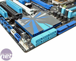
Down the bottom, the P55 SATA ports are neatly arranged along the edges of the PCB, with an extra three neatly placed along the bottom. The IDE slot will no doubt cause our almost militant "anti-IDE" community few to spit fire, but for a mainstream solution it's still expected. Unfortunately since the Marvell SATA 6Gbps controller screw up, Asus has had to turn to JMicron for the extra three SATA ports.
They make for a strange mix and it's hard to tell what is connected to what to use the "DriveXpert" feature that Asus premiered with its P45 Deluxe, and continues to use here. If you want to shoot to the SATA performance page, you'll see why you want to avoid these for everything bar optical drives, but even then, they are positioned far too low for opticals that typically sit in the top of a case.

MSI MPG Velox 100R Chassis Review
October 14 2021 | 15:04




Want to comment? Please log in.