
With the announcement of the Republic Of Gamers product line, Asus has been making some changes to its enthusiast line of motherboards in recent months. The first in Asus’ new line was the Crosshair, based on NVIDIA’s nForce 590 SLI chipset for socket AM2 Athlon 64 processors – we will be publishing our thoughts on that board very soon. There are a few layout issues with the Crosshair, but there are several unique features on the board too.
We have been working closely with Asus for the last couple of weeks, testing its latest addition to the Republic Of Gamers product line. The Striker Extreme is based on NVIDIA’s all new flagship nForce 680i SLI chipset, designed for Intel’s Core 2 based processors. The Striker carries over many of the unique features found on the Crosshair – but before we delve into it, we’re going to go through some of the basics of NVIDIA’s new chipset.
Many were waiting for the anticipated arrival of NVIDIA’s nForce 590 SLI Intel Edition chipset, but it was heavily delayed from its initial July launch plan, with limited retail boards only turning up in October. NVIDIA went incredibly quiet on the chipset front, and some partners canned their nForce 590 SLI Intel Edition projects in readiness for NVIDIA’s next chipset – nForce 680i SLI.
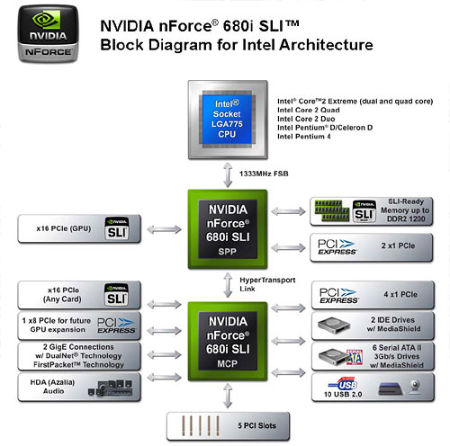
nForce 680i SLI Block Diagram
When designing nForce 680i SLI, NVIDIA wanted to alleviate the shortcomings of its previous Core 2 chipsets and make something that enthusiasts and overclockers would crave. However, don’t be fooled into thinking that nForce 680i SLI is a completely new product – it inherits the nForce 590 SLI Intel Edition Media Communication Processor, MCP55, and all of its features.
With that said, though, MCP55 is the most feature-rich south bridge available – it comes complete with six SATA 3Gbps ports, a single PATA port, ten USB 2.0 ports, dual PHY Gigabit Ethernet and support for High-Definition Audio. If you want a full run down of all of the features on the nForce 590 SLI southbridge, you can check out Wil’s nForce 500-series chipset overview.
Although the south bridge brings nothing new to the table, nForce 680i SLI’s north bridge (System Platform Processor, or SPP) – codenamed C55 – does bring some new goodness to the table. It’s the first NVIDIA chipset to natively support DDR2-800 memory and up to 1200MHz using NVIDIA’s SLI Memory initiative. It also adds support for a 1333MHz front side bus for when Intel unveils processors supporting the increased front side bus speed.
Along with these improvements, NVIDIA has engineered its nForce 680i SPP with extreme overclocking in mind. Although the chipset has support for future Intel processors supporting a 1333MHz front side bus speed, you will be able to achieve front side bus speeds well in excess of this with a bit of overclocking. The independent memory clock also includes support for NVIDIA Quicksync Technology. Here’s a quote from NVIDIA, describing the way data synchronisation works:
“Typically, the FSB and memory are connected together with logic that resembles a gearbox; this logic is designed to gradually synchronize data from one clock domain to another. Unfortunately, the gearbox logic typically adds latency to returning data, which can affect an overclock negatively. NVIDIA Quicksync bypasses this gearbox logic when Sync Mode is active.”
Quicksync essentially accelerates the return of data to the CPU from the memory when the front side bus and memory buses are running in Sync Mode. Quicksync is enabled when the memory ratio setting is set to “Linked” – this sets both the memory and front side buses to the same base clock speed, although it’s worth remembering that the memory bus runs at DDR (double data rate), while the front side bus is quad-pumped (QDR).
We have been working closely with Asus for the last couple of weeks, testing its latest addition to the Republic Of Gamers product line. The Striker Extreme is based on NVIDIA’s all new flagship nForce 680i SLI chipset, designed for Intel’s Core 2 based processors. The Striker carries over many of the unique features found on the Crosshair – but before we delve into it, we’re going to go through some of the basics of NVIDIA’s new chipset.
NVIDIA nForce 680i SLI Overview:
NVIDIA’s previous ‘Intel Edition’ chipsets have been renowned for their poor overclocking capabilities. In fact, many enthusiasts have been crying out for a Core 2 chipset with decent overclocking features and support for NVIDIA’s esteemed SLI technology.Many were waiting for the anticipated arrival of NVIDIA’s nForce 590 SLI Intel Edition chipset, but it was heavily delayed from its initial July launch plan, with limited retail boards only turning up in October. NVIDIA went incredibly quiet on the chipset front, and some partners canned their nForce 590 SLI Intel Edition projects in readiness for NVIDIA’s next chipset – nForce 680i SLI.
nForce 680i SLI Block Diagram
When designing nForce 680i SLI, NVIDIA wanted to alleviate the shortcomings of its previous Core 2 chipsets and make something that enthusiasts and overclockers would crave. However, don’t be fooled into thinking that nForce 680i SLI is a completely new product – it inherits the nForce 590 SLI Intel Edition Media Communication Processor, MCP55, and all of its features.
With that said, though, MCP55 is the most feature-rich south bridge available – it comes complete with six SATA 3Gbps ports, a single PATA port, ten USB 2.0 ports, dual PHY Gigabit Ethernet and support for High-Definition Audio. If you want a full run down of all of the features on the nForce 590 SLI southbridge, you can check out Wil’s nForce 500-series chipset overview.
Although the south bridge brings nothing new to the table, nForce 680i SLI’s north bridge (System Platform Processor, or SPP) – codenamed C55 – does bring some new goodness to the table. It’s the first NVIDIA chipset to natively support DDR2-800 memory and up to 1200MHz using NVIDIA’s SLI Memory initiative. It also adds support for a 1333MHz front side bus for when Intel unveils processors supporting the increased front side bus speed.
Along with these improvements, NVIDIA has engineered its nForce 680i SPP with extreme overclocking in mind. Although the chipset has support for future Intel processors supporting a 1333MHz front side bus speed, you will be able to achieve front side bus speeds well in excess of this with a bit of overclocking. The independent memory clock also includes support for NVIDIA Quicksync Technology. Here’s a quote from NVIDIA, describing the way data synchronisation works:
“Typically, the FSB and memory are connected together with logic that resembles a gearbox; this logic is designed to gradually synchronize data from one clock domain to another. Unfortunately, the gearbox logic typically adds latency to returning data, which can affect an overclock negatively. NVIDIA Quicksync bypasses this gearbox logic when Sync Mode is active.”
Quicksync essentially accelerates the return of data to the CPU from the memory when the front side bus and memory buses are running in Sync Mode. Quicksync is enabled when the memory ratio setting is set to “Linked” – this sets both the memory and front side buses to the same base clock speed, although it’s worth remembering that the memory bus runs at DDR (double data rate), while the front side bus is quad-pumped (QDR).


MSI MPG Velox 100R Chassis Review
October 14 2021 | 15:04

Want to comment? Please log in.