
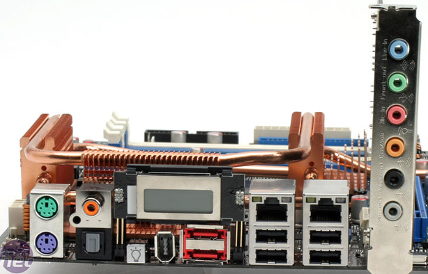
Rear I/O:
The Striker Extreme has an incredibly unique rear I/O panel, unlike anything we’ve ever seen before. There are a plethora of devices and ports that make up the rear I/O panel, with the most notable inclusion being an LCD display that can help with POST failure diagnosis. Typically motherboard manufacturers have included POST LED diagnosis displays, but unfortunately those require a list in order to decode the hex code displayed on the readout.While the LCD display isn’t in an optimal position (it’d be better on the motherboard somewhere or as a desktop LCD: ala Abit's 3rd Eye in our opinion), it does give you a lot more information and doesn’t require a list of error codes in order to work out exactly what the board is trying to tell you. Regardless of the fact that we don’t like the positioning of the device, we can’t help but love the idea behind it.
To the left of the LCD display there are the co-axial and optical S/PDIF out ports, along with the obligatory PS/2 ports. Underneath the LCD there is the “light switch” we mentioned on the previous page, along with an IEEE1394a Firewire port and a pair of eSATA 3Gbps ports controlled by a Silicon Image 3132 disk controller. To the right there are two Gigabit Ethernet ports, with four USB 2.0 ports directly below them. Further right, we’ve plugged the Asus SupremeFX Audio card, which provides 7.1 channel High-definition surround-sound.
BIOS:
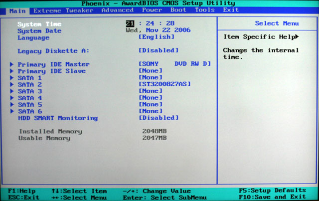
Asus uses a custom version of the Phoenix AwardBIOS on the Striker Extreme – the version we have used is 0403, but bear in mind that our board is a pre-production engineering sample. There are a couple of quirky bugs that Asus is trying to fix, but this early revision BIOS should give you an idea of what the final BIOS will look like when the board goes on general sale next month.Highlights:
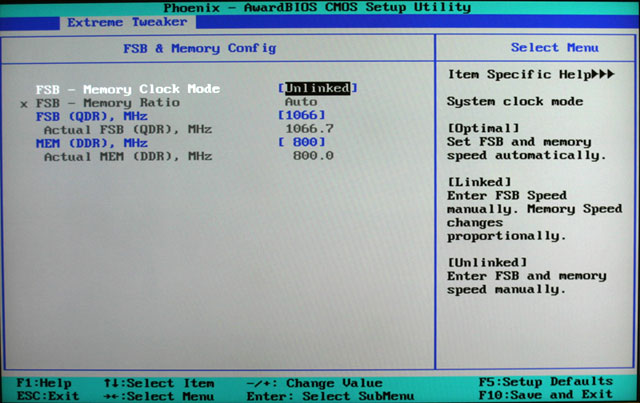
- Front Side Bus (QDR): 533-3000MHz in 1MHz increments;
- Memory Clock (DDR): 400-2000MHz in 1MHz increments;
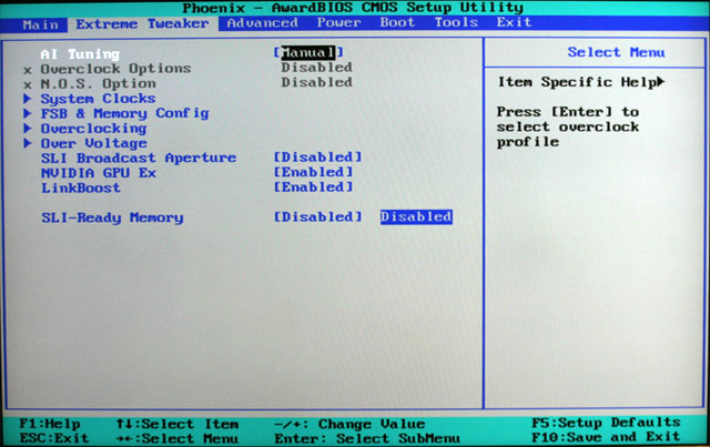
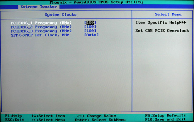
- PCI-Express Frequency: independent adjustment on each of the three PCI-Express x16 slots from 100-200MHz in 1MHz increments;
- DDR2 Voltage: adjustable from 1.800V (auto) to 3.425V in 0.025V increments;
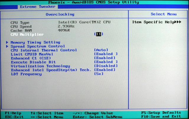
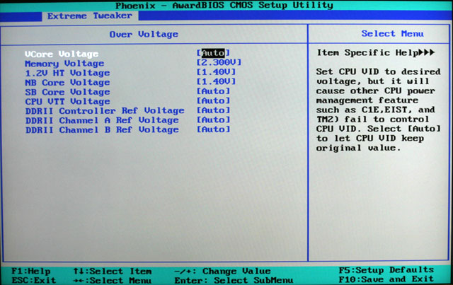
- CPU Voltage: adjustable from 0.83125V to 1.90000V in 0.00625V increments;
- Additional Voltage Adjustment: 1.2V HT Voltage, NB Core Voltage, SB Core Voltage, CPU VTT Voltage, DDRII Controller Ref Voltage, DDRII Channel A Ref Voltage, DDRII Channel B Ref Voltage;
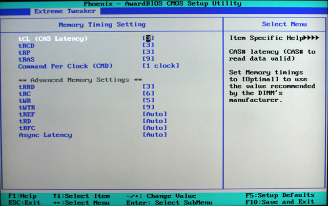
- Memory Timings: tCL (CAS Latency), tRCD (Row Address to Column Address Dela), tRP (Row Precharge), tRAS (Row Active Strobe), Command Per Clock (CMD), tRRD (Row to Row Delay), tRC (Row Cycle Time), tWR (Write to Read Delay), tWTR (Internal Write to Read Command Delay), tREF (Refresh Rate), tRD (Read Delay), tRFC (Row Cycle Refresh Time) and Async Latency.
Click to enlarge
Speaking of front side bus speeds, this has to be the highest selectable front side bus speed I’ve ever seen. You can select up to 3000MHz QDR (Quad data-rate) in 1MHz increments – that’s 750MHz with a 0.25MHz granularity when considering actual clock frequencies. In much the same way, the memory clock is selectable all the way up to 2600MHz, although you’ll be pushed to find DDR2 memory capable of that kind of frequency.
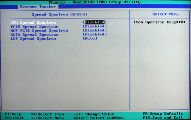
Each of the three PCI-Express x16 slots has individual frequency control from 100-200MHz, while the SPP to MCP reference clock can be raised from 200MHz to 500MHz should that be required (probably not – Ed.). Voltage control is equally incredibly comprehensive. Memory voltage can be adjusted all the way up to 3.425V in 0.025V increments, while CPU voltage is almost equally insane, with a maximum voltage of 1.90000V and a 0.00625V granularity all the way down to 0.83125V.
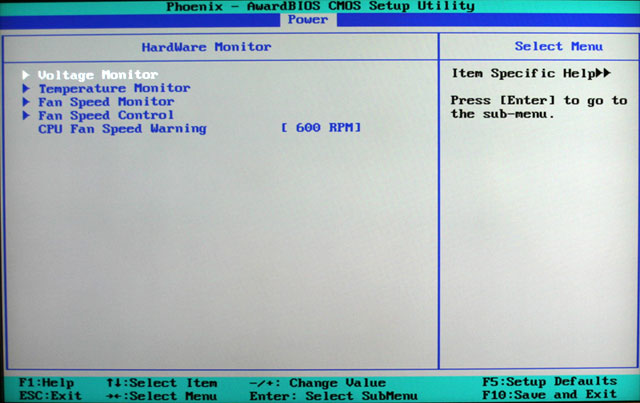
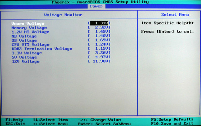
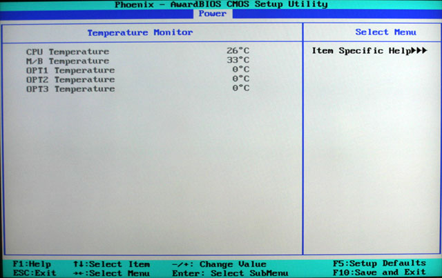
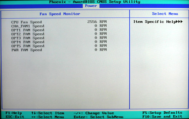
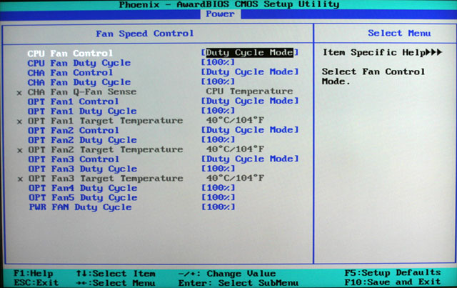
There is a sense of over-engineering that breathes through the Striker Extreme’s BIOS – Asus also includes comprehensive fan control, fan monitoring, voltage monitoring and (of course) temperature monitoring. The BIOS is just incredible and is easier to navigate than the traditional Asus BIOS layout we’ve become accustomed to over the years. Awesome.


MSI MPG Velox 100R Chassis Review
October 14 2021 | 15:04

Want to comment? Please log in.