Built for enthusiasts, by enthusiasts...?
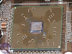
Today, ATI is announcing its entry into the market of enthusiast orientated chipsets for AMD users with the launch of its CrossFire Xpress 3200 platform. Over the last year, ATI has made a pretty big entrance into the chipset market as a major contender with market share increasing three-fold over that time period. That must've been helped by Intel's decision to choose ATI's Radeon Xpress 200M chipset for its entry-level integrated graphics motherboard, along with the launch of RD480, CrossFire and the Radeon X1000-series video cards.The new chipset, codenamed RD580, is said to deliver the world's best gaming performance, best overclocking capabilities and unparalleled stability. We've put ASUS's A8R32-MVP Deluxe through our usual bout of gruelling stress and performance testing, but before we get to that, we'll explain what ATI has done to create a chipset that has had enthusiasts in mind from the outset.


Back in December, we reported that Sami Maekinen - who is known by many as Macci - joined ATI's motherboard team to help the firm make a product that is designed to capture enthusiasts and overclockers because of its insane overclocking abilities. In order to make this possible, ATI's ASIC team - headed by John Bruno - have massively overspecced all logic inside the chipset.
One of the key overspecification factors is worst case silicon corner, meaning that there's no need to over-volt the silicon in order to achieve incredible overclocking results. Along with that, the HyperTransport link and PCI-Express interface have both been optimised so they can run massively over the specified limits. ATI has also removed internal clock divisions too, meaning that increasing the reference HyperTransport clock means that internal clock speeds are increased by the same one-to-one ratio. All of these should result in larger performance benefits when overclocking your system.

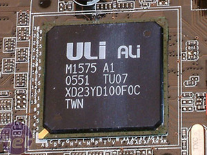
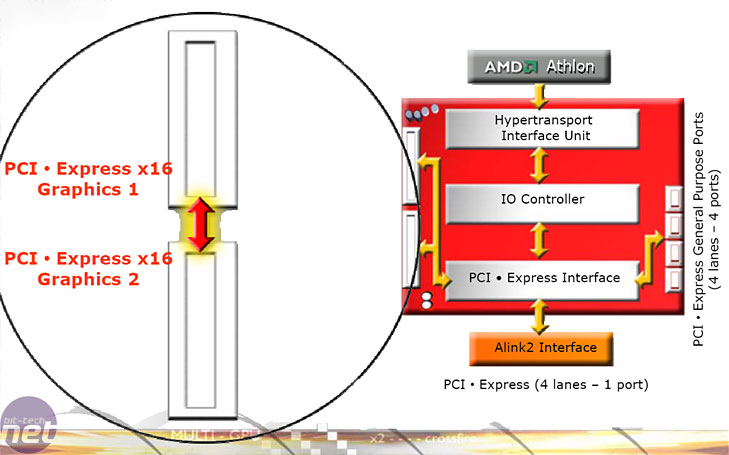
The remaining four ports are used to connect the North Bridge to the South Bridge - this is known as the Alink2 Interface. As a result of this, RD580 can support pretty much any South Bridge that runs on the PCI-Express interface - this is why there's a picture of the preferred ULi M1575 South Bridge at the top of the page.
Over the last twelve months or so, we have spent a long time chatting with ATI's motherboard partners about their collective short and long term plans with ATI's chipset products. A lot of them were sceptical about the I/O performance of the current ATI South Bridge, along with the lack of support for forward-looking features like SATA II. Due to these misdemeanours, many of ATI's partners opted for the pin-compatible and more feature-rich ULi M1575 South Bridge until the next-generation ATI South Bridge is released later this year.

MSI MPG Velox 100R Chassis Review
October 14 2021 | 15:04


Want to comment? Please log in.