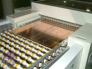
After the copper plating process has been completed, it is time to start working on the outer PCB layer. The manufacturing process that we have followed is for a four-layer PCB. ECS has the capacity for up to six layers in this particular factory. Before the PCB is laminated, it undergoes some chemical pre-treatment.
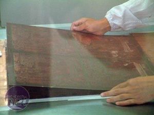
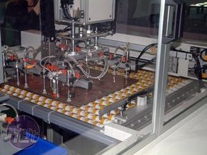
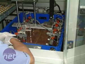
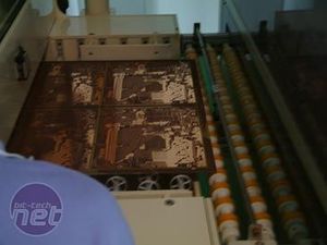
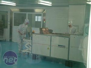
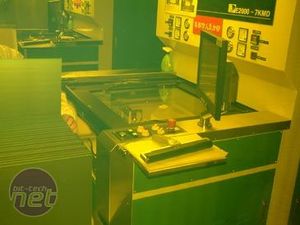
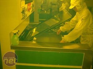
Once the lamination process is completed on both sides of the PCB, both sides go through an Alignment Exposure Unit. This machine basically photographs both sides of the PCB, allowing closer inspections of the circuitry to be completed before etching.



Want to comment? Please log in.